Transient storage circuit suitable for CMOS integration and using method thereof

A circuit and storage unit technology, applied in the field of radio frequency identification, can solve problems such as the decline of identification efficiency

Active Publication Date: 2012-07-18
BEIJING TONGFANG MICROELECTRONICS
View PDF0 Cites 0 Cited by
  • Summary
  • Abstract
  • Description
  • Claims
  • Application Information

AI Technical Summary

Problems solved by technology

It can effectively solve the problem of low identification efficiency caused by short-term power failure of the tag chip in passive radio frequency identification applications, reduce the time cost of tag identification, and improve the identification efficiency of passive radio frequency tags. It is economical and simple.

Method used


Image

  • Transient storage circuit suitable for CMOS integration and using method thereof
  • Transient storage circuit suitable for CMOS integration and using method thereof
  • Transient storage circuit suitable for CMOS integration and using method thereof

Examples


Embodiment 1

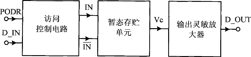
[0075] see Figure 2 to Figure 4 and Figure 10 to Figure 14 , The transient storage circuit of the present invention is composed of an access control circuit, a transient storage unit and an output sensitive amplifier connected in sequence. The reset signal PODR and the input data signal D_IN of the digital circuit of the tag chip are written into the transient storage unit through the access control circuit, and the temporary storage data output Vc of the transient storage unit is amplified by the output sensitive amplifier and then output by the data line D_OUT. According to the reset mode of the reset signal, the access control circuit is one of the following two structures:

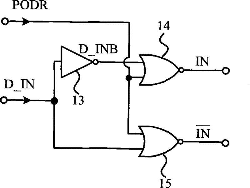
[0076] 1) The reset signal PODR is valid for high level reset and digital system for normal operation at low level. The input data signal D_IN is respectively connected to one input terminal of NOR gate 2 15 and connected to NOR gate 1 14 via inverter 1 13 One input end of NOR gate 14 and the other...

Embodiment 2

[0095] see Figure 5 to Figure 14 , The transient storage circuit of the present invention is composed of an access control circuit, a transient storage unit and an output sensitive amplifier connected in sequence. The reset signal PODR, input data signal D_IN and write enable signal WEN of the digital circuit of the label chip are written into the transient storage unit through the access control circuit, and the temporary storage data output Vc of the transient storage unit is amplified by the output sensitive amplifier and then amplified by the data Line D_OUT output. According to the reset mode of the reset signal, the access control circuit is one of the following four structures:

[0096] 1) When the reset signal PODR is high, the reset is valid, and when the low level is low, the chip works normally. When the write enable signal WEN is low, it is valid to write to the transient storage circuit. When WEN is high, the transient storage circuit is in the data transient st...


PUM


Abstract

The invention discloses a transient storage circuit suitable for CMOS integration and a using method thereof, which relate to the technical field of radio frequency identification (RFID). The transient storage circuit consists of an access control circuit, a transient storage unit and an output sensitive amplifier which are connected with one another in turn. A reset signal PODR and an input datasignal D IN of a digital circuit of a tag chip are written into the transient storage unit by the access control circuit, and the temporary data output Vc of the transient storage unit is amplified by the output sensitive amplifier and then is output by a data wire D_OUT. The transient storage circuit can solve the problem of lowered identification efficiency caused by short time power down of the tag chip in application of passive radio-frequency identification, reduces the time cost for tag identification, improves the identification efficiency of a passive radio-frequency tag, and has the characteristics of economical efficiency, simplicity and convenience.

Description

technical field [0001] The invention relates to the technical field of radio frequency identification (RFID), in particular to a transient memory suitable for CMOS integration of a radio frequency tag chip in a passive radio frequency identification system and a use method thereof. Background technique [0002] Radio frequency identification technology is a non-contact automatic identification technology, which uses radio frequency signals and spatial coupling transmission characteristics to realize automatic identification of identified targets. Passive electronic tags have become a research hotspot in the field of radio frequency identification in recent years due to their outstanding advantages such as small size, light weight, low cost, long life, and portability. see figure 1 The passive radio frequency identification tag 1 with transient storage function is composed of five parts: antenna and matching circuit, radio frequency front-end module, digital baseband process...

Claims


Application Information

Patent Timeline
Patent Type & Authority Patents(China)
IPC IPC(8): G11C14/00G06K19/07
Inventor 马长明吴行军
Owner BEIJING TONGFANG MICROELECTRONICS
Why Eureka
Try Eureka