Capacitance measurement circuit and capacitance measurement method
A capacitance measurement, capacitance technology, applied in the direction of measuring electrical variables, measuring resistance/reactance/impedance, measuring devices, etc.
- Summary
- Abstract
- Description
- Claims
- Application Information
AI Technical Summary
Problems solved by technology
Method used
Image

Examples
no. 1 example
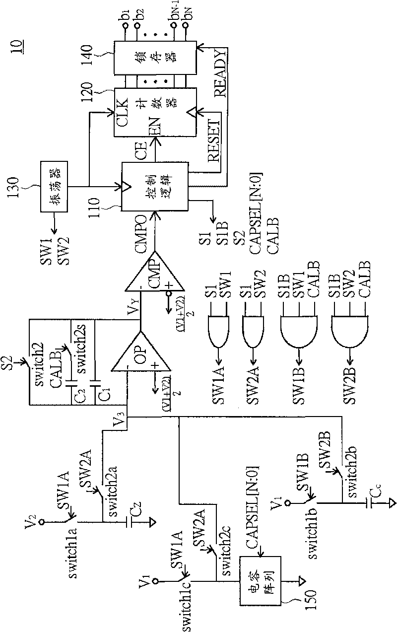
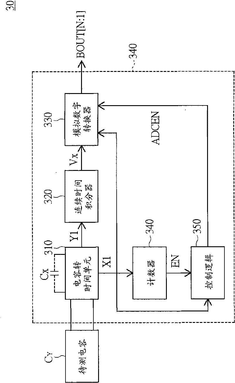
[0058] Please also refer to Figure 4 , 5 , 6, 7 and 8, Figure 4 and 5 Partial detailed circuit diagrams of the capacitance measuring circuit are shown respectively, Figure 6 shows a detailed circuit diagram of the capacitance variable circuit, Figure 7 shows the signal timing diagram of the first embodiment, Figure 8 A schematic diagram of an analog-to-digital converter is shown. The aforementioned capacitance measurement circuit 30 can selectively operate during the capacitance value setting period or the capacitance value measurement period. The capacitance measurement circuit 30 can preferably adjust the equivalent capacitance value of the adjustable variable capacitance Cx in advance during the capacitance value setting period, so that the capacitance measurement circuit 30 can more accurately measure the capacitance C to be measured during the capacitance value measurement period. Y .
[0059] The capacitance-to-time unit 310 includes an adjustable capacitance...
no. 2 example
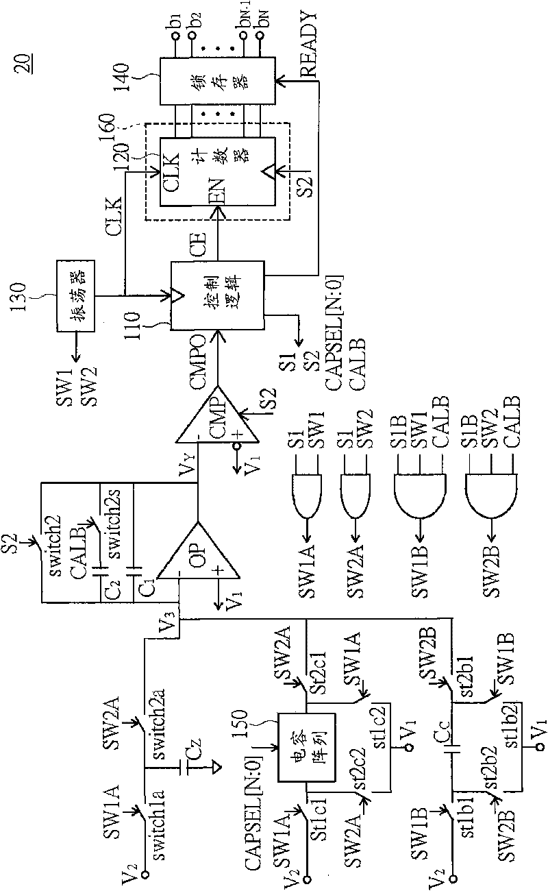
[0084] Please also refer to Figure 9 and Figure 10 , Figure 9 shows a partial detailed circuit diagram of the capacitance measuring circuit of the second embodiment, Figure 10 A signal timing chart of the second embodiment is shown. The difference between the second embodiment and the first embodiment lies in that the design of the current source 414 of the second embodiment is different from that of the current source 314 of the first embodiment. In addition to the operational amplifier OP1, the n-channel metal-oxide-semiconductor (NMOS) transistor LN1 as a switch, the p-channel metal-oxide-semiconductor (PMOS) transistors LP1 and LP2 as a switch, and the resistor Rb, the current source 414 also includes a switch The p-channel metal oxide semiconductor (PMOS) transistor LP2A. The current source 414 makes the current flow through the capacitor under test C Y It is K times different from the current of the adjustable variable capacitor Cx. In this way, the adjustable ...
no. 3 example
[0086] Please also refer to Figure 11 , which shows a partial detailed circuit diagram of the capacitance measuring circuit of the third embodiment. The difference between the third embodiment and the first embodiment lies in that the design of the current source 514 of the third embodiment is different from that of the current source 314 of the first embodiment. Current source 514 divides operational amplifier OP1, n-channel metal-oxide-semiconductor (NMOS) transistor LN1 as a switch, p-channel metal-oxide-semiconductor (PMOS) transistor LP1 as a switch, p-channel metal-oxide-semiconductor (PMOS) transistor as a switch In addition to the transistor LP2 and the resistor Rb, a transistor array 5142 is also included. The transistor array 5142 is controlled by the current setting signal ISEL[N:0] to provide K times the current I2.
[0087] Please refer to Figure 12 , which shows a detailed circuit diagram of the transistor array. The transistor array 5142 includes transisto...
PUM
 Abstract
Description
Claims
Application Information
 - R&D
- Intellectual Property
- Life Sciences
- Materials
- Tech Scout
- Unparalleled Data Quality
- Higher Quality Content
- 60% Fewer Hallucinations
Browse by: Latest US Patents, China's latest patents, Technical Efficacy Thesaurus, Application Domain, Technology Topic, Popular Technical Reports.
© 2025 PatSnap. All rights reserved.Legal|Privacy policy|Modern Slavery Act Transparency Statement|Sitemap|About US| Contact US: help@patsnap.com