

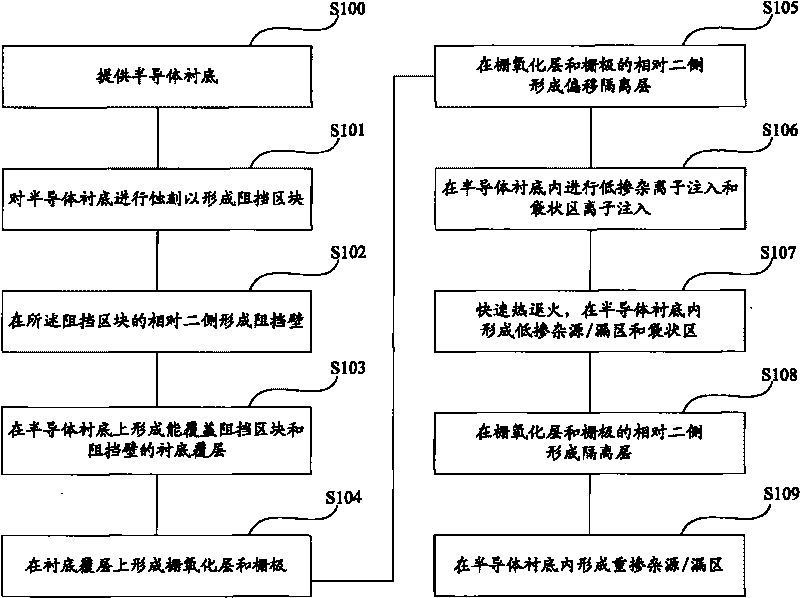
Semiconductor device and manufacture method thereof
A manufacturing method and semiconductor technology, applied in the direction of semiconductor devices, semiconductor/solid-state device manufacturing, electrical components, etc., can solve problems such as deterioration, punch-through effect electrical performance, etc.
- Summary
- Abstract
- Description
- Claims
- Application Information
AI Technical Summary
Problems solved by technology
Method used
Image

Examples
Embodiment Construction
[0027] The inventors found that because the existing MOS transistors use ultra-shallow junction technology to make the source / drain region in order to overcome the short channel effect, but the implanted ions in the source / drain region will cause diffusion and penetration, which will cause the source / drain region Junction capacitance and junction leakage lead to punch-through effect between source / drain regions, affecting the quality of MOS transistors.
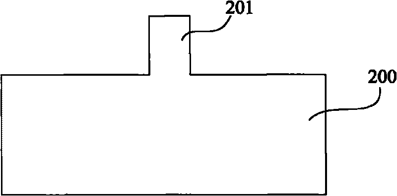
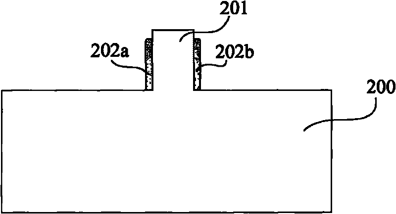
[0028] Therefore, in the manufacture of semiconductor devices, in order to prevent the occurrence of the above-mentioned defects. In the present invention, the provided semiconductor substrate is firstly etched to form a barrier block; barrier walls are formed on opposite sides of the barrier block; a substrate covering capable of covering the barrier block and the barrier wall and integrated with the semiconductor substrate is formed. layer, the barrier wall has a drop from the surface of the substrate cladding layer; a gate...
PUM
| Property | Measurement | Unit |
|---|---|---|
| Thickness | aaaaa | aaaaa |
Abstract
Description
Claims
Application Information