Ion implantation zone forming method, MOS transistor and manufacture method thereof

A technology for MOS transistors and ion implantation regions, which is applied in semiconductor/solid-state device manufacturing, semiconductor devices, electrical components, etc., and can solve the problems of source/drain region overflow or punch-through electrical performance, deterioration, etc.

Active Publication Date: 2012-12-19
SEMICON MFG INT (SHANGHAI) CORP +1
View PDF0 Cites 0 Cited by
  • Summary
  • Abstract
  • Description
  • Claims
  • Application Information

AI Technical Summary

Problems solved by technology

[0006] The problem solved by the present invention is: in the manufacturing process of semiconductor devices, how to improve the junction capacitance and junction leakage in the short channel effect, and avoid the problems of overflow or punch-through between the source / drain regions and the deterioration of electrical performance

Method used


Image

  • Ion implantation zone forming method, MOS transistor and manufacture method thereof
  • Ion implantation zone forming method, MOS transistor and manufacture method thereof
  • Ion implantation zone forming method, MOS transistor and manufacture method thereof

Examples


Embodiment Construction

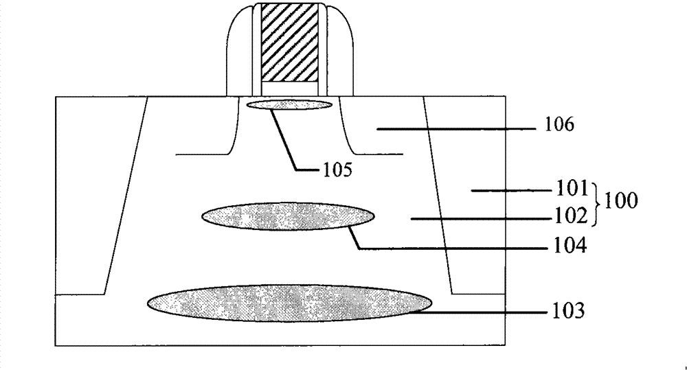
[0030] The inventors found that, because the existing MOS transistors use ultra-shallow junction technology to form source / drain regions to overcome the short channel effect, but the implanted ions in the source / drain regions will cause diffusion and penetration, which will cause the source / drain regions Junction capacitance and junction leakage lead to overflow or punch-through effect between source / drain regions, affecting the electrical quality of MOS transistors.

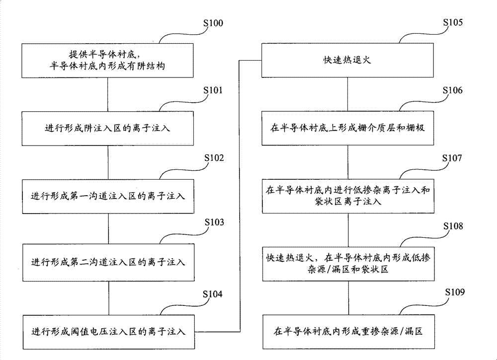
[0031] Therefore, when manufacturing MOS transistors, in order to prevent the occurrence of the above-mentioned defects. In the present invention, the ion implantation process is carried out in the well structure of the semiconductor substrate in order to form the well implantation region, the first channel implantation region, the second channel implantation region and the threshold voltage implantation region, wherein the second The channel implantation region is located between the source / drain regions to be ...


PUM

PropertyMeasurementUnit
thicknessaaaaaaaaaa

Abstract

The invention discloses an ion implantation zone forming method, an MOS transistor and a manufacture method thereof, wherein the ion implantation zone forming method comprises the following methods: carrying out the ion implantation for forming a trap implantation zone; carrying out the ion implantation for forming a first groove implantation zone; carrying out the iron implantation for forming asecond groove implantation zone which is positioned between source / drain zones to be formed; carrying out iron the implantation for forming a threshold voltage implantation zone; and carrying out thermal annealing treatment. The invention additionally forms the groove implantation zones between the source / drain zones in a semiconductor substrate, effectively baffles the mutual penetration betweenthe source / drain zones, improves the short groove effect of semiconductor devices, avoids the overrun effect and the punch-through effect between the source / drain zones, improves the electric performance of the semiconductor devices, and simultaneously provides a larger process regulation space for the reduction of junction capacitance in the ultra shallow junction process and the expansion of a process window.

Description

technical field [0001] The invention relates to the technical field of semiconductor manufacturing, in particular to a method for forming an ion implantation region in a well structure, a MOS transistor and a manufacturing method thereof. Background technique [0002] Metal-oxide-semiconductor (MOS) transistors are the main driving force as semiconductor devices move toward high density and small size. The driving current and hot carrier injection are the two most important parameters in the design of MOS transistors. The traditional design obtains the expected performance by controlling the doping shape of the gate dielectric layer, channel region, well region, source / drain extension region, pocket implant (Pocket Implant) region, source / drain region implant shape and thermal budget, etc. . [0003] As the channel length of the MOS device becomes shorter, the depletion regions of the source / drain regions are too close to each other, which will lead to undesired punch-thro...

Claims


Application Information

Patent Timeline
Patent Type & Authority Patents(China)
IPC IPC(8): H01L21/336H01L21/265H01L29/78H01L29/10
Inventor 赵猛
Owner SEMICON MFG INT (SHANGHAI) CORP
Why Eureka
Try Eureka