Thin film transistor array substrate as well as application and manufacturing method thereof

A technology of thin-film transistors and array substrates, applied in the fields of thin-film transistor array substrates and their application and manufacturing, can solve problems such as error prone, image sticking, and affecting the display function of liquid crystal display panels, etc., to expand the display viewing angle and reduce alignment The effect of the error problem

Active Publication Date: 2010-06-16
INNOLUX CORP
View PDF5 Cites 31 Cited by
  • Summary
  • Abstract
  • Description
  • Claims
  • Application Information

AI Technical Summary

Problems solved by technology

[0005] However, when the above-mentioned CF substrate and TFT array substrate are combined in alignment, errors are likely to occur in the alignment between the CF substrate and the TFT array substrate, thus affecting the display function of the assembled liquid crystal display panel, such as optical transmittance or Response time may also lead to unstable alignment of liquid crystal molecules, resulting in image sticking

Method used


Image

  • Thin film transistor array substrate as well as application and manufacturing method thereof
  • Thin film transistor array substrate as well as application and manufacturing method thereof
  • Thin film transistor array substrate as well as application and manufacturing method thereof

Examples


Embodiment Construction

[0057]In order to make the above and other objects, features, advantages and embodiments of the present invention more comprehensible, this description will list a series of embodiments for illustration. However, it should be noted that these examples are only used to illustrate the implementation of the present invention, rather than to limit the present invention.

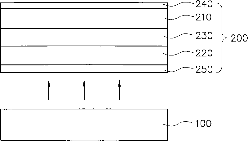
[0058] refer to figure 1 , which represents a schematic cross-sectional view of the liquid crystal display device according to the first embodiment of the present invention. The liquid crystal display device of this embodiment includes a backlight module 100 and a liquid crystal display panel 200 . The liquid crystal display panel 200 is arranged above the backlight module 100, and the backlight module 100 can be an edge-light (Edge Lighting) backlight module or a direct-down (Bottom Lighting) backlight module to provide backlight to the liquid crystal display panel 200, wherein the backlight module 100 is pref...


PUM


Abstract

The invention discloses thin film transistor array substrate as well as application and manufacturing method thereof. The manufacturing method comprises at least the following steps of: providing a substrate; forming a plurality of thin film transistors on the substrate; forming a plurality of first pixel electrodes on the substrate; forming an electrode insulating layer on the first pixel electrodes; and forming a plurality of second pixel electrodes on the electrode insulating layer. The thin film transistor array substrate can be used in a liquid crystal display panel or a liquid crystal display device.

Description

technical field [0001] The invention relates to a thin film transistor array substrate and its application and manufacturing method, and in particular to a thin film transistor array substrate capable of forming liquid crystal multi-domain alignment effect and its application and manufacturing method. Background technique [0002] As the information and communication industries continue to innovate, the liquid crystal display (Liquid Crystal Display; LCD) market is booming. Liquid crystal displays have the advantages of high image quality, small size, light weight, low driving voltage and low power consumption, etc., so they are widely used in personal digital assistants (Personal Digital Assistant; PDA), mobile phones, camcorders, notebooks, etc. Consumer communication or electronic products such as computers, desktop monitors, car monitors and projection TVs. [0003] Generally speaking, a liquid crystal display panel mainly includes a color filter (Color Filter; CF) subs...

Claims


Application Information

Patent Timeline
Patent Type & Authority Applications(China)
IPC IPC(8): H01L27/12H01L21/84G02F1/1362
Inventor 谢志勇陈建宏陈建诚
Owner INNOLUX CORP
Why Eureka
Try Eureka