
Liquid crystal display device

A technology of a liquid crystal display device and a display part, which is applied in the direction of nonlinear optics, instruments, optics, etc., can solve the problems of not being able to fully ensure the uniformity of the gap, the injection of liquid crystals, etc., and achieve a reliable light-shielding effect

Active Publication Date: 2013-11-13
NEC LCD TECH CORP
View PDF4 Cites 0 Cited by
  • Summary
  • Abstract
  • Description
  • Claims
  • Application Information

AI Technical Summary

Problems solved by technology

Therefore, the two substrates come into contact, and the uniformity of the gap and the injection of liquid crystals cannot be sufficiently ensured in this part, and there are problems such as the generation of air bubbles.

Method used


Image

  • Liquid crystal display device
  • Liquid crystal display device
  • Liquid crystal display device

Examples


Embodiment 1

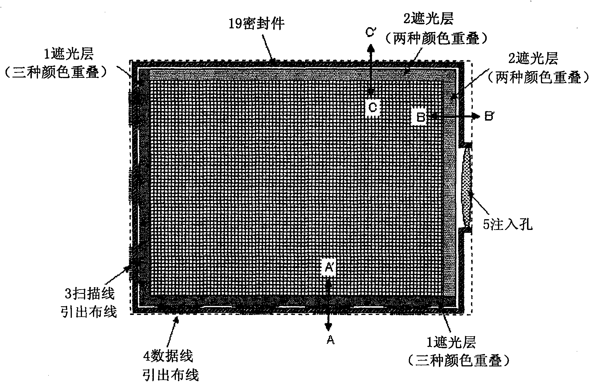
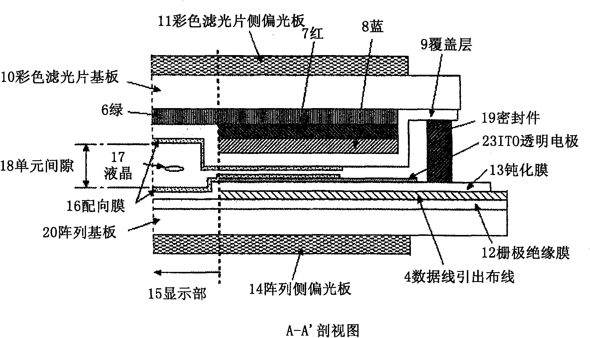
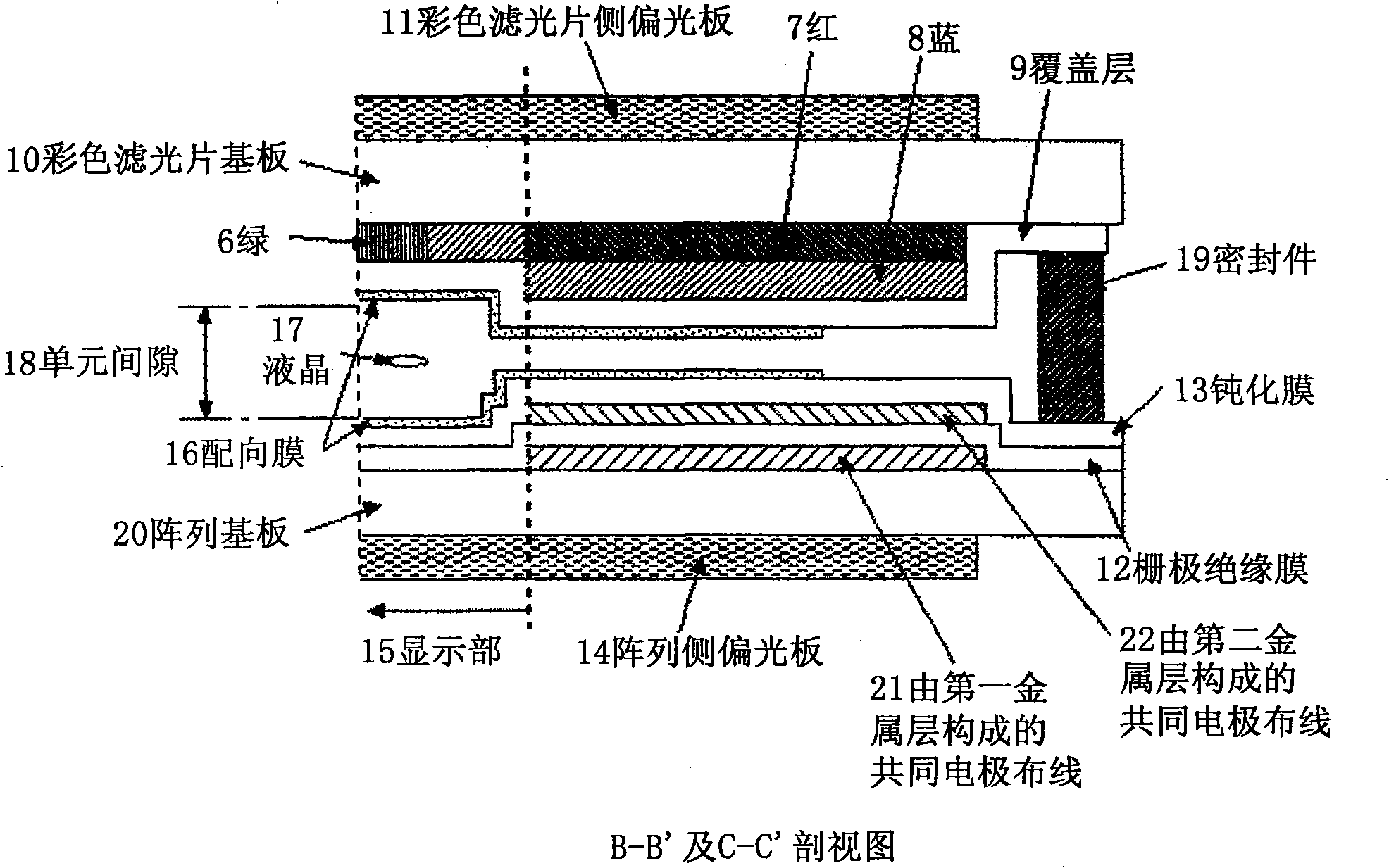
[0033] In order to describe in more detail an embodiment of the present invention described above, refer to Figure 1 to Figure 3 . FIG. 8 illustrates an active matrix liquid crystal display device according to a first embodiment of the present invention. figure 1 It is a top view of the active matrix liquid crystal display device of this embodiment. figure 2 for figure 1 A cross-sectional view of the A-A' portion, image 3 for figure 1 The cross-sectional view of the B-B' portion. 8( a ) is a plan view showing a schematic structure of electrodes on the array substrate, and FIG. 8( b ) is an enlarged view of the region shown in 8( a ).

[0034] Such as figure 2As shown, the liquid crystal display device of this embodiment has: an array substrate 20 with an array pattern in which pixels including switching elements such as TFT (Thin Film Transistor, thin film transistor) are arranged in a matrix; a color filter opposite to the array substrate 20 A sheet substrate 10; a ...

Embodiment 2

[0066] Next, refer to Figure 4 to Figure 6 , an active matrix liquid crystal display device according to a second embodiment of the present invention will be described. Figure 4 It is a top view showing the frame structure of the active matrix liquid crystal display device of the present embodiment, Figure 5 for Figure 4 A cross-sectional view of the A-A' portion, Image 6 for Figure 4 A cross-sectional view of the B-B' portion, Figure 7 for Figure 4 The cross-sectional view of the C-C' portion of .

[0067] Such as Figure 4As shown, compared to Embodiment 1, only the side with the scan line lead-out wiring 3 and the side with the data line wiring 4 are formed as a light-shielding layer 1 in which the three colors of RGB overlap. In this embodiment, on this basis, On the side opposite to the side with the data line lead-out wiring 4, a light-shielding layer 1 overlapping three colors of RGB is formed, and only on the frame edge of the remaining side is formed by...


PUM


Abstract

A normally-black active-matrix-type liquid crystal display device comprises a first substrate having color layers of three or more colors and a second substrate on which an active-matrix array is formed. The first substrate has a structure, which is devoid of a black matrix, in which the color layers are stacked in a frame portion surrounding the display area. A first light-shielding layer in which color layers of three of more colors are stacked is formed on the frame portion on a side of the display area from which scanning lines are led out and on a side of the display area from which data lines are led out, from among four sides of the display area. A second light-shielding layer in which color layers of two colors are built up is formed on the frame portion on at least one side of the other remaining sides of the display area.

Description

technical field [0001] The present invention relates to an active matrix liquid crystal display device, in particular to an active matrix liquid crystal display device having a light-shielding structure in which a black matrix is ​​replaced by stacking color layers. Background technique [0002] In recent years, there has been a strong demand for an equipment structure and a manufacturing process capable of manufacturing an active matrix liquid crystal display device with good display quality at a lower cost. [0003] For example, in a liquid crystal display device, in order to block the light incident from the frame edge, a metal such as chromium (chromium oxide) or resin is used on the side of the substrate having a color filter (color filter substrate) to form a black color called black. A light-shielding layer of a matrix (BM: Black Matrix), but for the purpose of cost reduction, a technique of omitting the black matrix has been proposed. [0004] For example, Patent Do...

Claims


Application Information

Patent Timeline
Patent Type & Authority Patents(China)
IPC IPC(8): G02F1/1335
CPCG02F1/1362G02F1/133512
Inventor 西田真一高桥聪之助渡边贵彦坂口嘉一川崎拓
Owner NEC LCD TECH CORP
Learn More