Packaging method and packaging structure of light emitting diode (LED) module

A packaging method and display module technology, applied in the direction of identification devices, instruments, electrical components, etc., can solve the problems of increasing manufacturing costs, affecting the first pass rate of LED display modules, separation, etc., to improve manufacturing quality, improve first pass rate, The effect of reducing manufacturing costs

Active Publication Date: 2012-01-04
JIANGSU WENRUN OPTOELECTRONICS
View PDF0 Cites 4 Cited by
  • Summary
  • Abstract
  • Description
  • Claims
  • Application Information

AI Technical Summary

Problems solved by technology

Since the epoxy resin 3 is firmly connected to the circuit board 2 and the LED chip 4 after curing, once the circuit board 2 or the LED chip 4 is damaged, it cannot be separated from the epoxy resin 3
The irreparability of existing LED display modules affects the first pass rate of LED display modules and increases their manufacturing costs

Method used


Image

  • Packaging method and packaging structure of light emitting diode (LED) module
  • Packaging method and packaging structure of light emitting diode (LED) module
  • Packaging method and packaging structure of light emitting diode (LED) module

Examples


Embodiment Construction

[0018] The present invention will be further described below in conjunction with drawings and embodiments.

[0019] Such as figure 1 , figure 2 Shown, packaging method of the present invention comprises the following steps:

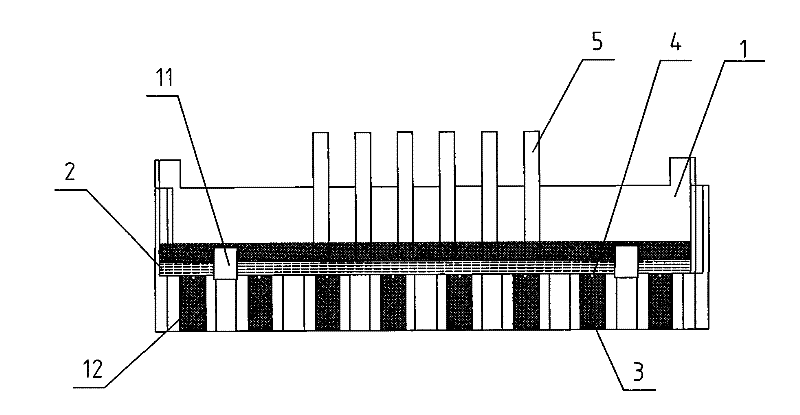
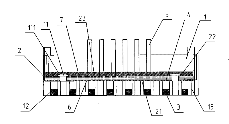
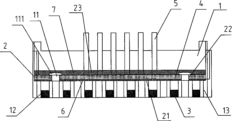
[0020] 1) Turn the display module cavity 1 upside down, inject epoxy resin 3 into each glue injection hole 12 on the panel of the display module cavity 1 with a syringe or other dispensing equipment, and pour the epoxy resin 3 with a thickness equal to the depth of the glue injection hole 12 1 / 2, bake and solidify;

[0021] 2) A plurality of LED chips 4 are bonded to the front surface 21 of the circuit board 2 with a die-bonding glue, and the first layer of silicone resin 6 is sprayed on the surface to form a transparent protective layer, which is baked and solidified;

[0022] 3) Put the circuit board 2 into the cavity 1 of the display module with the first layer of silicone resin 6 facing down and the pins 5 facing up, so that the pair of positionin...


PUM


Abstract

The invention relates to a packaging method and a packaging structure of a light emitting diode (LED) module. The invention discloses a packaging method of an LED display, which comprises the following steps of: (1) injecting epoxy resin with the depth half of that of a resin injection hole into each resin injection hole of a cavity panel of a display module; (2) spraying a first layer of silica gel resin on the front face of a circuit board; (3) sleeving a location hole on the circuit board on a location column of the cavity of display module, and abutting the surface of the first layer of silica gel against the inner side face of the cavity panel of the display module; (4) ironing out the upper end of the location column protruding out of the back of the circuit board to form a nut cap;and (5) pouring a second layer of silica gel resin on the back of the circuit board. The invention also discloses a packaging structure using the method, comprising the cavity of the display module, the circuit board and a plurality of LED wafers, wherein the LED wafers are respectively located in the corresponding resin injection holes. In the invention, the inner stress of the epoxy resin in the resin injection holes is eliminated, and the deformation of the cavity of the LED display module is prevented. In addition, the wafers or the circuit board can be replaced in the manufacture process, thereby the first-time qualification rate is improved.

Description

technical field [0001] The invention relates to a packaging method of an LED module, and also relates to a packaging structure of the LED module packaged by the method, belonging to the technical field of lighting displays. Background technique [0002] LED (light-emitting diode) is a solid-state semiconductor device that can directly convert electricity into light. As a new type of energy-saving light source, it has the advantages of low energy consumption, long life, high brightness, and short response time. A plurality of LED dies can be combined into an LED digital module or a dot matrix module in a dot matrix arrangement, and a plurality of LED display modules can be combined into an LED display that can display digital or colorful images. At present, in terms of signal display, outdoor advertising and large-scale displays in public places, LED display screens are more and more widely used due to their advantages such as large screens and good display effects. Existing...

Claims


Application Information

Patent Timeline
Patent Type & Authority Patents(China)
IPC IPC(8): H01L21/50H01L25/075H01L21/56G09F9/33H01L33/54
Inventor 张宏庭
Owner JIANGSU WENRUN OPTOELECTRONICS
Why Eureka
Try Eureka