Anti-static protection structure and manufacturing method thereof

A technology of protection structure and manufacturing method, applied in circuits, electrical components, electrical solid devices, etc., can solve problems such as increasing production costs, and achieve the effect of preventing damage and reducing production costs

Active Publication Date: 2010-06-23
SHANGHAI HUAHONG GRACE SEMICON MFG CORP
View PDF0 Cites 7 Cited by
  • Summary
  • Abstract
  • Description
  • Claims
  • Application Information

AI Technical Summary

Problems solved by technology

[0003] In order to achieve the above goals, it is necessary to use an additional layer of photomask to define the metal silicide blocking area (silicide diffusion blocking), but this will require an additional photolithography plate, which increases the production cost

Method used


Image

  • Anti-static protection structure and manufacturing method thereof
  • Anti-static protection structure and manufacturing method thereof
  • Anti-static protection structure and manufacturing method thereof

Examples


Embodiment Construction

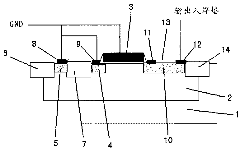
[0016] The invention discloses an antistatic protection structure, such as figure 2 As shown, it includes a P-type substrate 1 and a P well 2 on it. The P well 2 is provided with a first polysilicon gate 3, and the left side of the first polysilicon gate 3 is provided with a first N+ diffusion region 4, a P+ diffusion region 5 is also arranged on the left side of the first N+ diffusion region 4, a first field oxidation region 6 is arranged on the left side of the P+ diffusion region 5, and the P+ diffusion region 5 is connected to the first field oxidation region 5 A second field oxidation region 7 is separated between the first N+ diffusion regions 4, a first metal silicide 8 is arranged above the P+ diffusion region 5, and a second metal silicide is arranged above the first N+ diffusion region 4 9. The second metal silicide 9 is located on the left side of the first polysilicon gate 3, and the first metal silicide 8, the second metal silicide 9 and the first polysilicon gat...


PUM


Abstract

The invention discloses an anti-static protection structure. The right side of a first polysilicon gate is provided with a second polysilicon gate; a third metal silicide is arranged between the first polysilicon gate and the second polysilicon gate for partition; a second N+ diffusion region is arranged below the third metal silicide; a third N+ diffusion region is arranged below the right side of the second polysilicon gate; a second channel N-type diffusion region is arranged between the second polysilicon gate and the third N+ diffusion region; and a fourth metal silicide is arranged above the third N+ diffusion region. The invention also discloses a manufacturing method of the anti-static protection structure, the second polysilicon gate is manufactured while manufacturing the first polysilicon gate, before this, a N+ buried layer injection form is adopted or after this, the second channel N-type diffusion region is formed by transmitting the second polysilicon gate through an injection mode. The anti-static protection structure can effectively prevent the damage of the static electricity to devices, and simultaneously saves the manufacture of a mask of a metal silicide blocking area, thus reducing the production cost.

Description

technical field [0001] The invention relates to an antistatic protection structure, and also relates to a manufacturing method of the antistatic protection structure. Background technique [0002] The harm of static electricity to electronic products has always been a problem that is not easy to solve. The most used ESD protection structure today is the GGNMOS structure (Ground Gate NMOS, gate grounded NMOS). In order to improve the ESD protection capability of the output stage, a metal silicide blocking process technology has been developed in the process. The purpose is to remove the metal silicide in the NMOS components used in the output stage, and increase the sheet resistance of the drain and source. Larger, so that the MOS component has a higher drain resistance and source resistance, and a larger drain resistance and source resistance can effectively improve the protection ability of the MOS device against ESD. The existing GGNMOS antistatic structure such as figu...

Claims


Application Information

Patent Timeline
IPC IPC(8): H01L27/088H01L23/60H01L21/8234
Inventor 苏庆徐向明
Owner SHANGHAI HUAHONG GRACE SEMICON MFG CORP
Why Eureka
Try Eureka