Semiconductor package without outer pins and stacked structure thereof

A package and semiconductor technology, applied in the direction of semiconductor devices, semiconductor/solid-state device components, electric solid-state devices, etc., can solve problems such as improving defective products, short-circuiting wires, and complexity

Inactive Publication Date: 2010-06-30
ASE ASSEMBLY & TEST SHANGHAI
View PDF0 Cites 19 Cited by
  • Summary
  • Abstract
  • Description
  • Claims
  • Application Information

AI Technical Summary

Problems solved by technology

[0005] Although Figure 1B The single-chip quad flat no-lead package structure shown is beneficial to achieve high pin density packaging because it has multiple groups of contacts 112, but when the number of groups (that is, the number of rows) of the contacts 112 is greater than 4 groups or more When the wire bonding procedure of the wire 13 becomes complicated and difficult, that is, the wire 13 is too long, the bending points required for a single wire 13 increase, and the wire bonding between the wires 13 Technical problems such as complex staggered arrangement, which increase consumption cost and design difficulty
At the same time, during the molding process of the encapsulant 14, the flowing encapsulation material will easily push the overly long wires 13, causing the adjacent wires 13 to contact each other and cause a short circuit, thereby increasing the problem of defective products.
[0006] Therefore, it is necessary to provide a semiconductor package without external leads and its stacked structure to solve the high-density packaging problems existing when the existing quad flat no-lead (QFN) packaging technology is applied to the field of multi-chip modules

Method used


Image

  • Semiconductor package without outer pins and stacked structure thereof
  • Semiconductor package without outer pins and stacked structure thereof
  • Semiconductor package without outer pins and stacked structure thereof

Examples


Embodiment Construction

[0029] This embodiment will introduce the present invention in detail with reference to the drawings. The following descriptions of the various embodiments refer to the accompanying drawings to illustrate specific embodiments in which the present invention may be practiced. The direction terms mentioned in the present invention, such as "up", "down", "front", "rear", "left" or "right", etc., are only referring to the directions of the attached drawings. Therefore, the directional terms used are used to assist in explaining the relevant constructions, but not to limit the present invention.

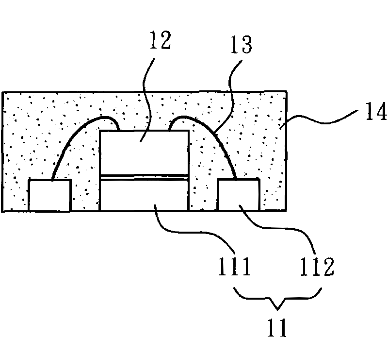
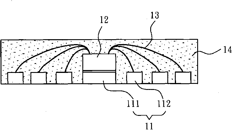
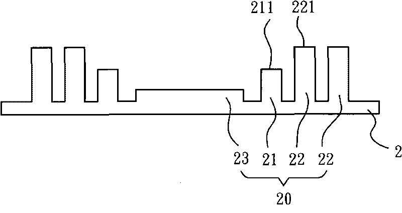
[0030] Please refer to Figure 2A , 2B, 2C, 2D and 2E, which disclose a schematic diagram of the manufacturing process of the semiconductor package without external leads and its stacked structure according to the first embodiment of the present invention, which is used to illustrate the non-leading semiconductor package of the first embodiment of the present invention. Possible manufac...


PUM


Abstract

The present invention discloses a semiconductor package without outer pins and a stacked structure thereof. A first package is formed by arranging at least one chip on a lead frame and carrying out a potting procedure. The two ends of a plurality of contacts are exposed out of the first package, so at least one second package is connected with one of the ends of the contacts. Thus, a POP (package on package) novel multi-chip module structure is made by taking the lead frame of a QFN (quad flat non-leaded) package structure as the base frame.

Description

【Technical field】 [0001] The present invention relates to a semiconductor package without external leads and its stacking structure, in particular to a quad flat no-lead (QFN) package for forming a package-on-package (POP) Constructs and their stacked constructs. 【Background technique】 [0002] Nowadays, in order to meet various high-density packaging requirements, the semiconductor packaging industry has gradually developed various types of packaging structures, among which various system in package (SIP) design concepts are often used to build high-density packaging structures. Generally speaking, system packaging can be divided into multi chip module (MCM), package on package (POP) and package in package (PIP). The multi-chip module (MCM) refers to arranging several chips on the same substrate. After setting the chips, all the chips are embedded with the same encapsulation gel, and can be subdivided into stacked chips ( stacked die) package or parallel chip (side-by-sid...

Claims


Application Information

Patent Timeline
Patent Type & Authority Applications(China)
IPC IPC(8): H01L25/00H01L23/488H01L23/495H01L23/31
CPCH01L2224/32145H01L2224/32245H01L2224/45147H01L2224/48091H01L2224/73265H01L2224/48247H01L2924/01047H01L2924/181H01L2224/45144H01L2924/00014H01L2924/00H01L2924/00012
Inventor 许宏达周若愚
Owner ASE ASSEMBLY & TEST SHANGHAI
Why Eureka
Try Eureka