Low-temperature transfer printing method used for microelectronically packaged carbon nanotube bumps

A technology of microelectronic packaging and carbon nanotubes, which is applied in the direction of circuits, electrical components, and electrical solid devices, and can solve problems such as the inability to meet the development requirements of high-density and miniaturization of electronic components, and large bump size and spacing. , to achieve the effect of reducing package size, high success rate transfer, and meeting high-density packaging

Inactive Publication Date: 2012-01-04
SHANGHAI UNIV
View PDF0 Cites 0 Cited by
  • Summary
  • Abstract
  • Description
  • Claims
  • Application Information

AI Technical Summary

Problems solved by technology

In recent years, bump technology in flip-chip soldering has developed rapidly, and solder bumps, indium bumps, gold bumps, and copper bumps have appeared successively. However, the size and spacing of these bumps are generally large, which cannot meet the electronic requirements. The development requirements of continuous high density and miniaturization of components

Method used


Image

  • Low-temperature transfer printing method used for microelectronically packaged carbon nanotube bumps
  • Low-temperature transfer printing method used for microelectronically packaged carbon nanotube bumps
  • Low-temperature transfer printing method used for microelectronically packaged carbon nanotube bumps

Examples


Embodiment 1

[0023] In this embodiment, the specific process and steps of the low-temperature transfer printing method of carbon nanotube bumps are as follows:

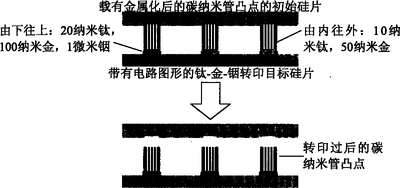
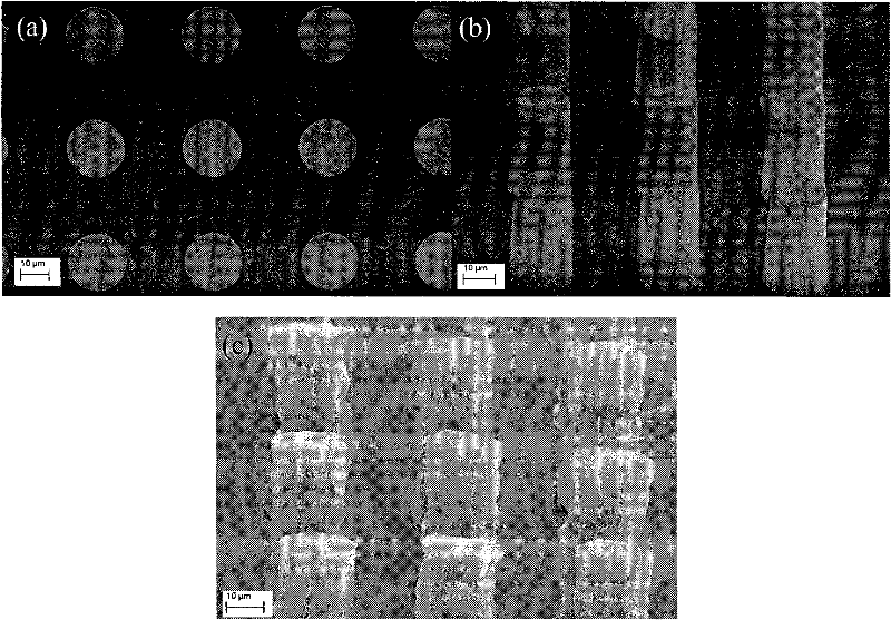
[0024] see figure 1 , figure 1 It is a schematic diagram of the transfer printing process for forming carbon nanotube bumps from carbon nanotube arrays in the present invention.

[0025] (1) First, a pattern array of 100×100 is engraved on the transfer target silicon wafer by ultraviolet lithography, each pattern is a circle with a diameter of 20 microns, and the distance between the circles is 40 microns.

[0026] (2) Using the sputtering method to sequentially deposit a titanium metal layer and a gold metal layer on the transfer target silicon wafer and the photoresist to form a conductive layer, wherein the thickness of titanium is 20 nanometers, and the thickness of gold is 100 nanometers.

[0027] (3) Deposit a transfer layer made of metal indium on the gold metal layer of the transfer target silicon wafer by electron beam ...


PUM

PropertyMeasurementUnit
thicknessaaaaaaaaaa
thicknessaaaaaaaaaa
thicknessaaaaaaaaaa

Abstract

The invention relates to a low-temperature transfer printing method used for microelectronically packaged carbon nanotube bumps, and belongs to the technical field of microelectronic device manufacturing processes. The transfer printing method comprises the following steps of: aligning to extrude a metallized silicon wafer of which the surface is provided with the carbon nanotube bumps by using atitanium-gold-indium transfer-printing objective silicon wafer with a circuit pattern at the temperature of between 170 and 200 DEG C and under the pressure of 107 pascals, and transferring the carbon nanotube bumps to the transfer-printing objective silicon wafer with the circuit pattern. The method can rapidly perform transfer printing on the carbon nanotube bumps at small intervals at relatively low temperature in a large area and at a high success rate so as to meet the requirements on concentration and miniaturization of electronic components, reduce the production cost and improve the production efficiency.

Description

technical field [0001] The invention relates to a low-temperature transfer printing method for carbon nanotube bumps used in microelectronic packaging, and belongs to the technical field of microelectronic device manufacturing technology. Background technique [0002] Flip-chip welding technology refers to attaching the chip with bumps face down directly on the substrate to realize the electrical, thermal and mechanical connection between the chip and the substrate. Compared with the traditional wire bonding technology, the flip-chip welding technology shortens the interconnection length, reduces the interconnection resistance and inductance, and greatly improves the electrical performance and high-frequency performance of the packaged device. Flip-chip welding technology is a high-density integrated circuit packaging technology, which improves the overall level of integrated circuit packaging technology and meets the needs of the development of the integrated circuit indust...

Claims


Application Information

Patent Timeline
Patent Type & Authority Patents(China)
IPC IPC(8): H01L21/603
CPCH01L2224/81
Inventor 刘建影
Owner SHANGHAI UNIV
Why Eureka
Try Eureka