Multi-layer printed circuit board machining process

A multi-layer circuit board and processing technology, which is applied in the direction of multi-layer circuit manufacturing, etc., can solve the problems of low residual copper rate, low alignment accuracy, and inconsistency of finished product size, so as to overcome the inaccurate alignment and high alignment. High precision and stability

Active Publication Date: 2010-07-14
SHENNAN CIRCUITS
View PDF0 Cites 16 Cited by
  • Summary
  • Abstract
  • Description
  • Claims
  • Application Information

AI Technical Summary

Problems solved by technology

However, due to the inconsistent stress parameters such as the material shrinkage rate of the substrate and the copper skin during the processing of the copper clad laminate, stress is generated between the copper skin and the substrate of the copper clad laminate.
Generally, the shrinkage or expansion coefficient of the substrate is relatively large, and the copper skin is relatively stable. The frame of the single flow glue point will have a low residual copper rate, and the shrinkage and expansion of the flow glue point frame with independent design will be relatively large, which will lead to internal wiring. Figure 1 is subject to the shrinkage pressure or expansion tension of the frame of the flow glue point, resulting in a large dislocation, that is, the expansion or contraction ratio of each layer of copper clad laminate may be different, which affects the alignment between the layers during the lamination process, so The alignment accuracy between the layers of the flow glue point frame is low
[0005] The frame of the large copper skin panel is to keep the copper skin 4 on the copper clad board outside the circuit pattern 1, or simply divide the copper skin 4 into several lar...

Method used


Image

  • Multi-layer printed circuit board machining process
  • Multi-layer printed circuit board machining process
  • Multi-layer printed circuit board machining process

Examples


Embodiment Construction

[0029] In order to describe the technical content, structural features, achieved goals and effects of the present invention in detail, the following will be described in detail in conjunction with the embodiments and accompanying drawings.
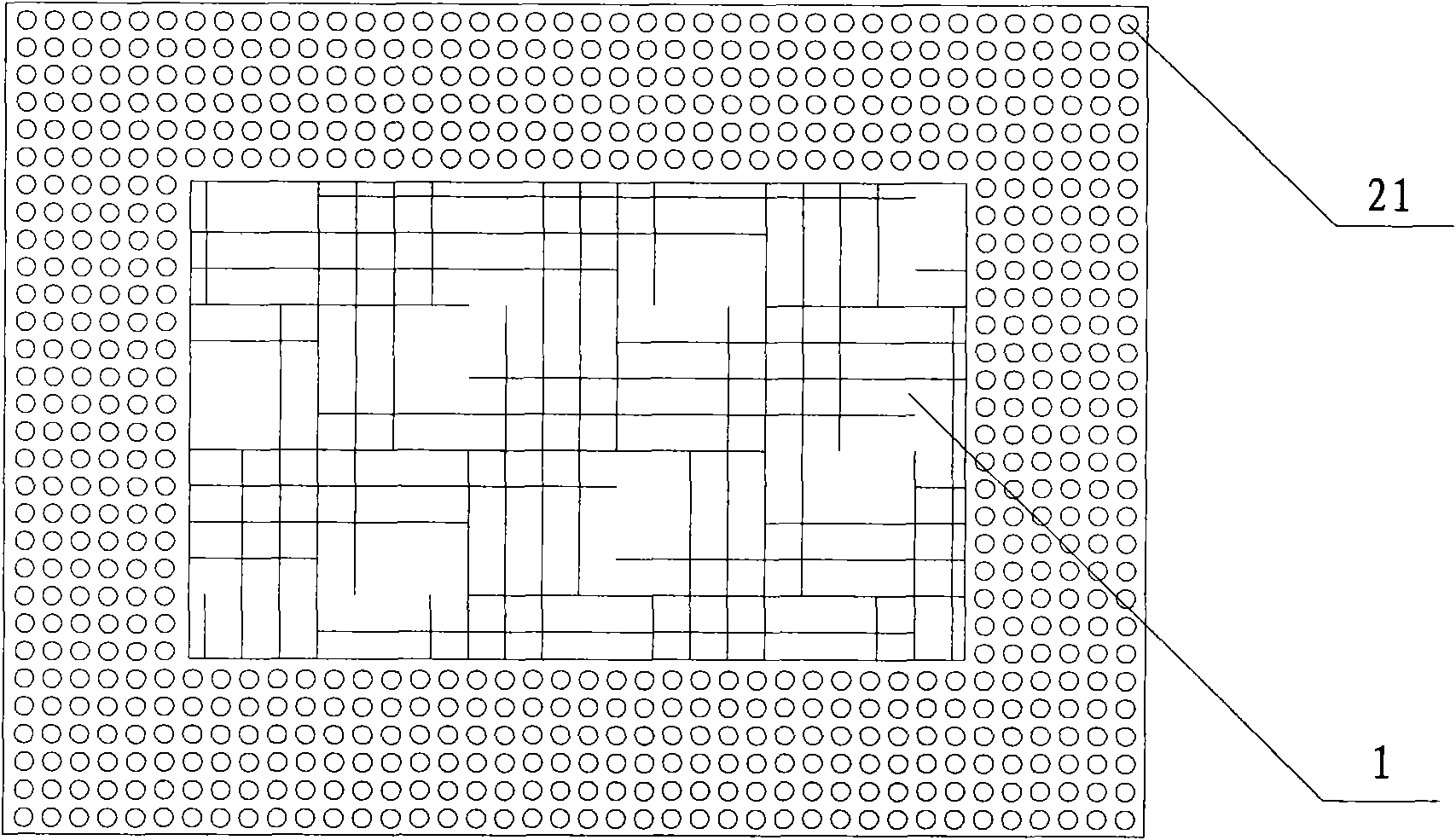
[0030] see image 3

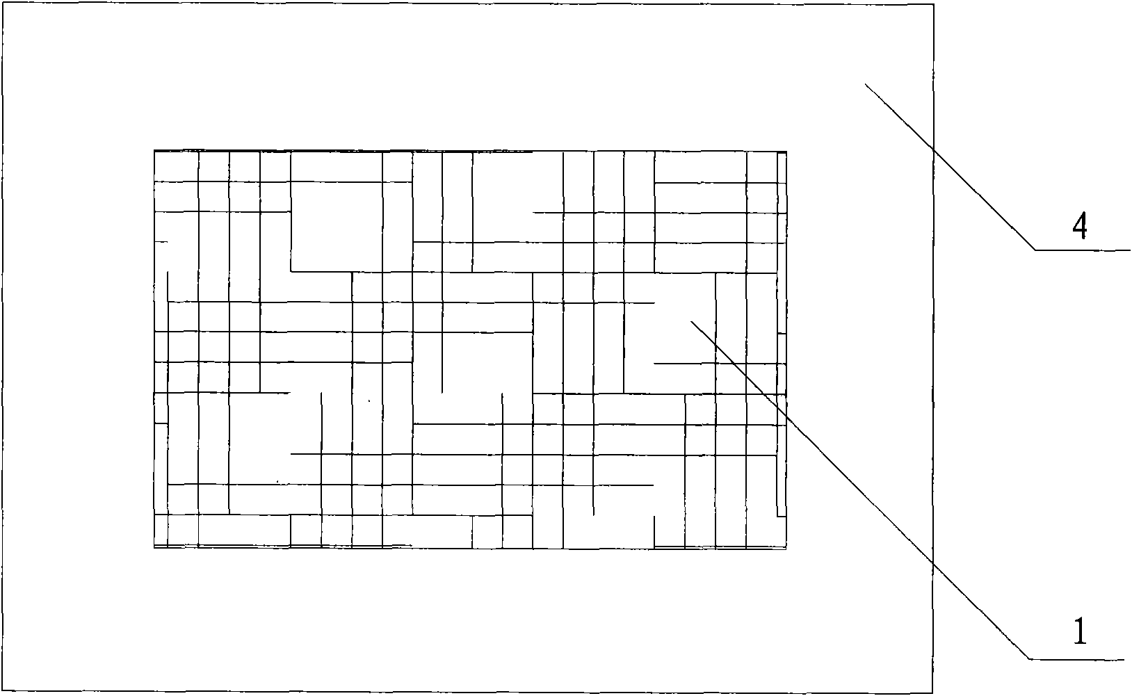
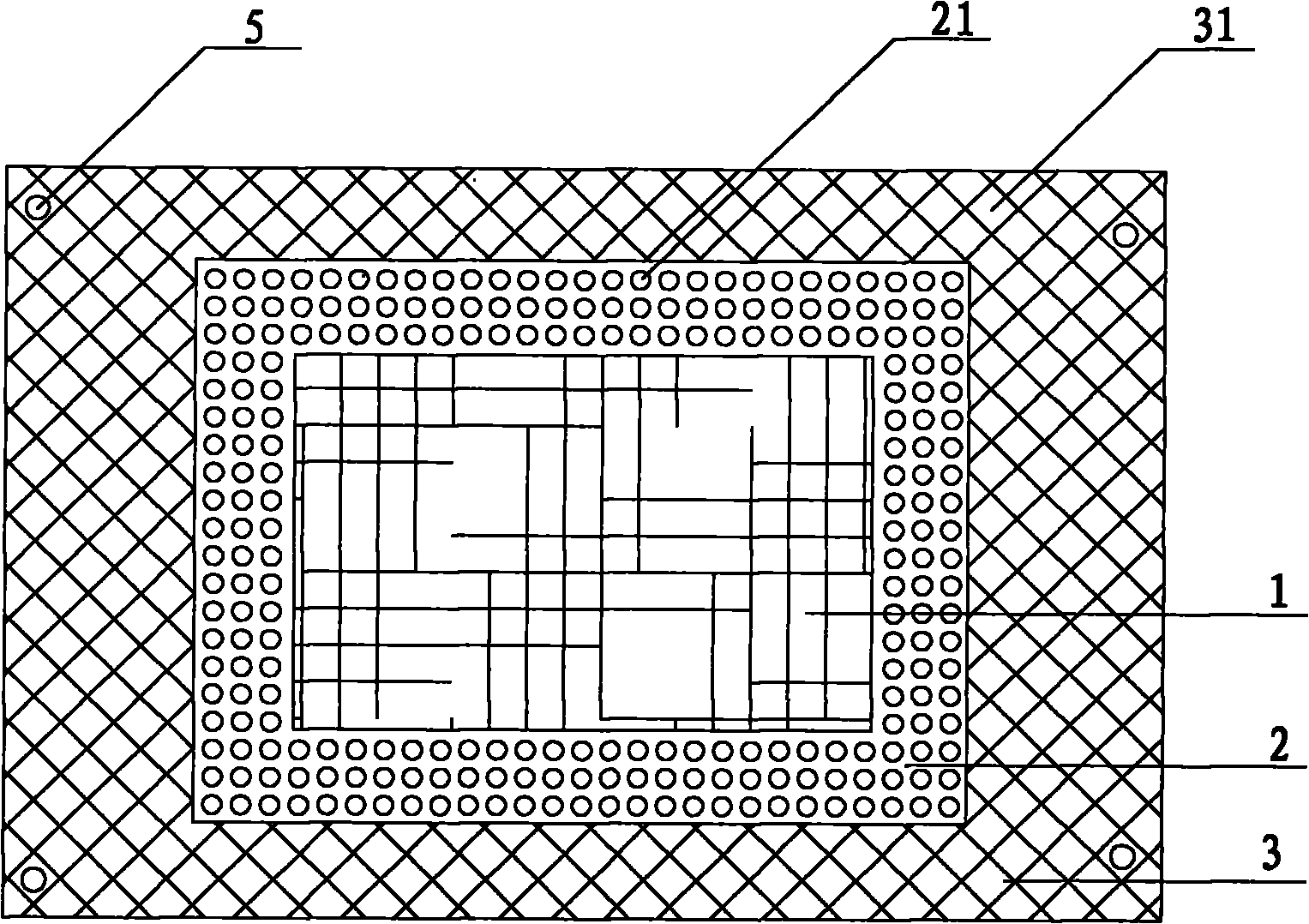
[0031] The multilayer printed circuit board processing technology provided in this embodiment includes the following steps in sequence:

[0032] 1) Make a line pattern 1 and a frame pattern on the copper clad laminate, the frame pattern is composed of a frame pattern I2 and a frame pattern II3, from the center area of ​​the copper clad laminate to the outside: line pattern 1, frame pattern I2, frame pattern II3 . The structure of the frame pattern I is a circular copper-clad point 21, and the exposed substrate is between the circular copper-clad points 21; between bare substrates. Among them, the interval between the circular copper clad points 21 is 0.5 mm to 1 mm, the diameter of the circular copper clad points ...


PUM

PropertyMeasurementUnit
Widthaaaaaaaaaa
Diameteraaaaaaaaaa

Abstract

The invention discloses a multi-layer printed circuit board machining process, which sequentially comprises the following steps: 1) manufacturing a circuit diagram and frame diagrams on a copper clad board, wherein the frame diagrams comprise a frame diagram I and a frame diagram II, the circuit diagram, the frame diagram I and the frame diagram II are sequentially arranged from the central zone of the copper clad board to the outside, and the copper residual rate of the frame diagram I is smaller than the copper residual rate of the frame diagram II; 2) laminating the copper clad board into a multi-layer circuit board, and milling off the outer edge of the multi-layer circuit board comprising the frame diagram II; 3) manufacturing a through hole, an outer diagram and a solder mask of the multi-layer circuit board; and 4) milling the multi-layer circuit board into the designed finished size. By adopting the machining process of the invention, the machining precision of the PCB is high, and the size of the PCB is accurate.

Description

technical field [0001] The invention relates to a processing technology of a printed circuit board, in particular to a processing technology of a multilayer printed circuit board. Background technique [0002] The current multilayer printed circuit board processing technology is to make graphics on the copper clad laminate, press it, and then mill out the frame. There are two main techniques: [0003] One is "glue dot jigsaw frame", and the other is "big copper skin jigsaw frame". [0004] Such as figure 1 The frame of glue-flow point assembly shown is outside the design pattern 1 of the copper-clad laminate, and the copper-clad surface other than the circuit pattern is made into circular copper-clad points 21, also called "glue-flow points". The circular copper-clad The copper skin other than point 21 is etched away to expose the substrate. Using the frame of the flow point is beneficial to avoid the shrinkage effect of the frame on the graphics in the board, and the ro...

Claims


Application Information

Patent Timeline
IPC IPC(8): H05K3/46
Inventor 黄立球吴志杰崔荣
Owner SHENNAN CIRCUITS
Why Eureka
Try Eureka