Grid electrode driving circuit unit, a grid electrode driving circuit and a display device

A gate drive circuit and drive unit technology, applied in static indicators, static memory, instruments, etc., can solve the problems of large layout area, large circuit power consumption, poor stability, etc., to reduce complexity, improve stability, Effect of Power Consumption Reduction

Inactive Publication Date: 2010-07-21
PEKING UNIV SHENZHEN GRADUATE SCHOOL +1
View PDF0 Cites 68 Cited by
  • Summary
  • Abstract
  • Description
  • Claims
  • Application Information

AI Technical Summary

Problems solved by technology

However, the gate drive circuit of this two-phase clock has obvious shortcomings: the power consumption of the circuit is large, the stability is poor, and the number of devices leads to complex circuits...

Method used


Image

  • Grid electrode driving circuit unit, a grid electrode driving circuit and a display device
  • Grid electrode driving circuit unit, a grid electrode driving circuit and a display device
  • Grid electrode driving circuit unit, a grid electrode driving circuit and a display device

Examples


Embodiment 1

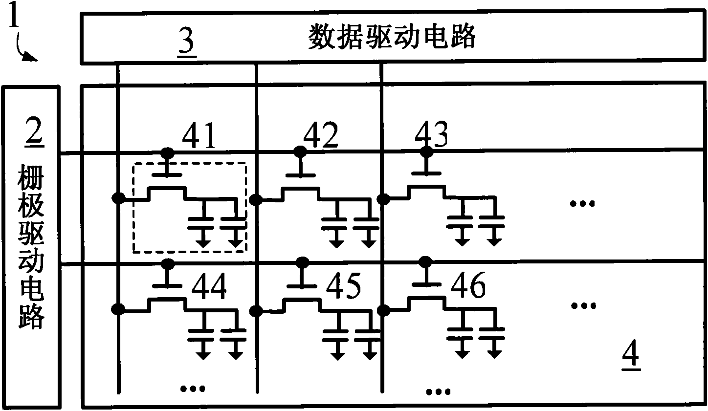
[0033] Such as figure 1 As shown, the display device 1 includes a panel 4 , a data driving circuit 3 and a gate driving circuit 2 . The panel 4 includes a two-dimensional pixel array composed of a plurality of pixels 41, 42, 43, 44, 46, 46, and a plurality of data lines in a first direction (for example, vertical direction) and a second data line connected to each pixel array. A plurality of gate scanning lines in a direction (for example, a horizontal direction). Usually, each gate scanning line corresponds to a row in the pixel array, and each data line corresponds to a column in the pixel array. The data driving circuit 3 is used to output image signals to the data lines; the gate driving circuit 2 is used to output driving signals to the gate scanning lines to complete the row scanning of the pixel array. The gate driving circuit can be connected to the panel by welding or the gate driving circuit can be integrated on the panel. The display device 1 may be a liquid crys...

Embodiment 2

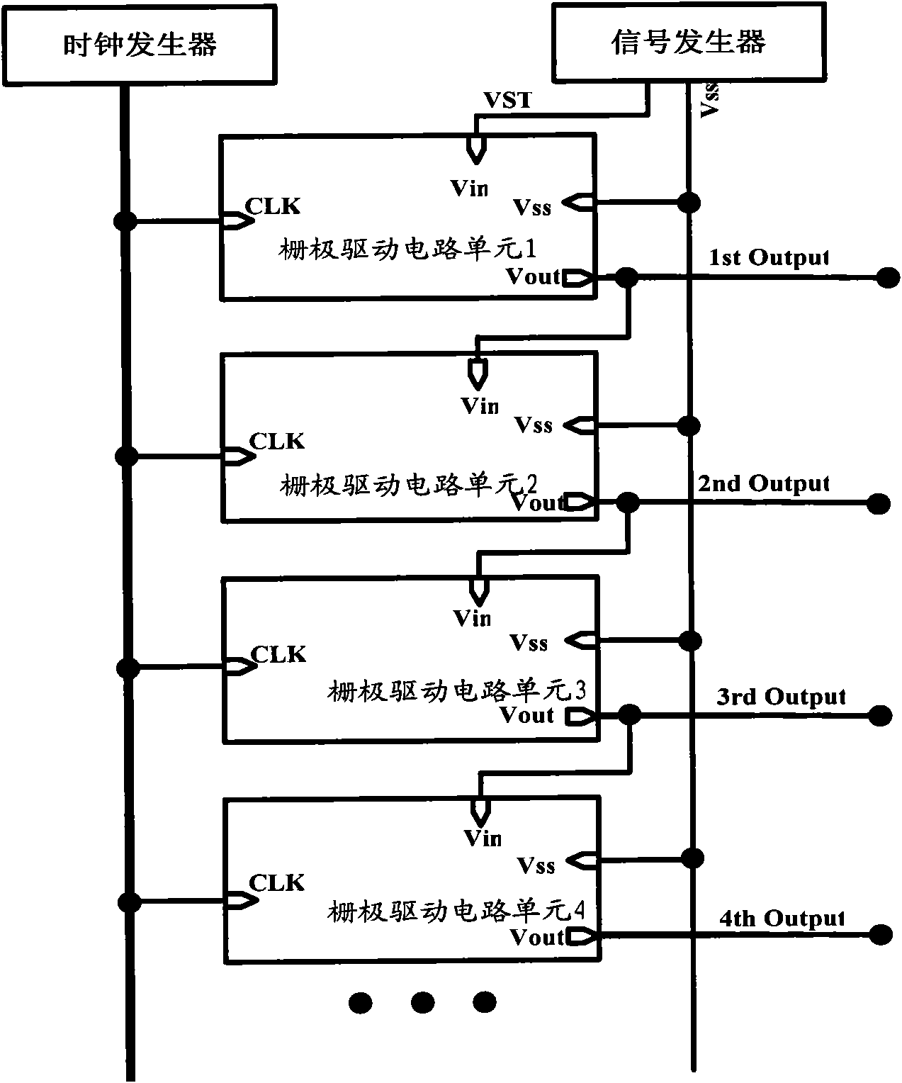
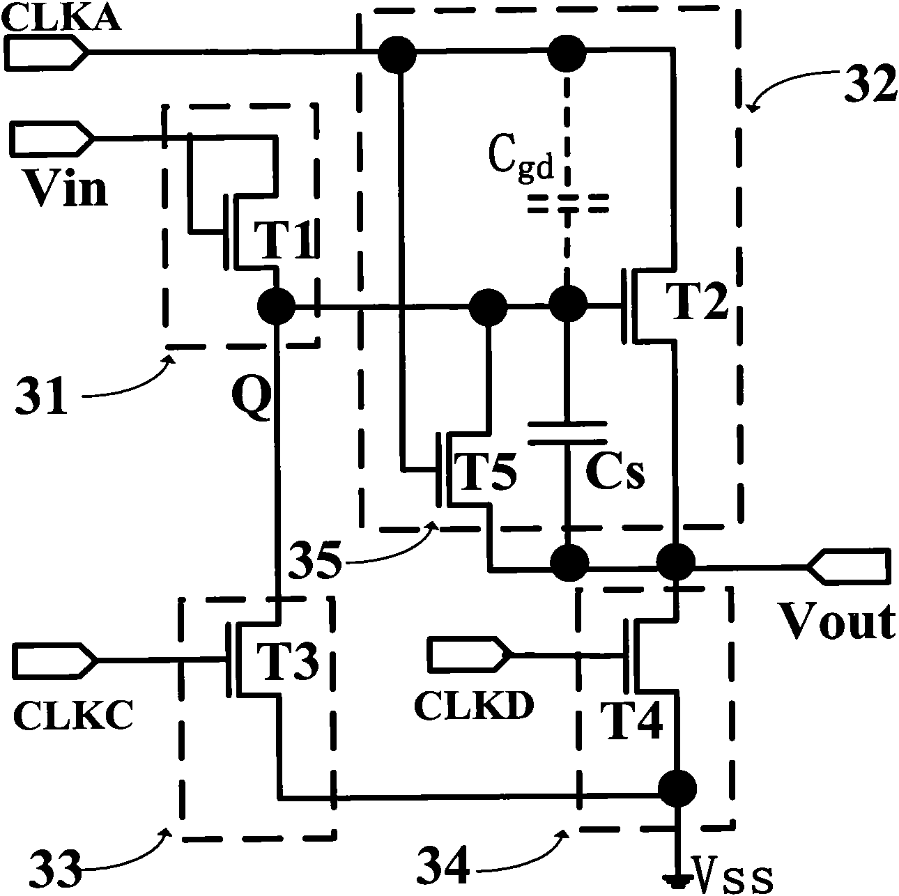
[0090] In another embodiment of the gate drive circuit unit, such as Figure 11 As shown, the gate drive circuit unit signal input interface, signal output interface, input signal control module, first clock signal control module, second clock signal control module, third clock signal control module and fourth clock signal control module. The signal input interface is used to receive the input pulse signal. If the gate drive circuit unit of this stage is the first stage, the input pulse signal is provided by the signal generator. If the gate drive circuit unit of the present stage is not the first stage, the input pulse signal Provided by the previous stage gate drive circuit unit. The signal output interface is used to output the driving signal to the corresponding scanning line and the signal input interface of the gate driving circuit unit of the next stage. The first clock signal control module includes a drive unit and a clock feedthrough suppression unit. The drive unit...


PUM


Abstract

The invention discloses a grid electrode driving circuit unit, a grid electrode driving circuit and a display device. The grid electrode driving circuit unit comprises a first clock signal control module, an input signal control module, a third clock signal control module and a fourth clock signal control module, wherein the first clock signal control module comprises a driving unit and a clock feed-through inhabiting unit, the driving unit transfers a first clock signal to an output port after being switched on, the clock feed-through inhabiting unit couples the control end of the driving unit to a signal output interface under the control of the first clock signal, the input signal control module provides the driving voltage for the driving unit under the control of an input pulse signal, the third clock signal control module provides the shutdown voltage for the driving unit under the control of a third clock signal, the third clock signal lags two phases behind the first clock signal, the fourth clock signal control module pulls down the voltage of the signal output interface under the control of a fourth clock signal, and the fourth clock signal is one phase ahead the first clock signal. The invention has the advantages of simple design, small power consumption and high stability.

Description

technical field [0001] The invention relates to a display device, in particular to a gate drive circuit of the display device. Background technique [0002] The amorphous silicon TFT process has the characteristics of low processing temperature, uniform device performance, low cost, and is suitable for large-area display. Therefore, the amorphous silicon TFT LCD process has become the mainstream of modern flat panel display technology. [0003] Gate drive circuit is an important part of amorphous silicon TFT LCD. In order to further improve the performance of amorphous silicon TFT LCD and reduce its cost, in recent years, the research of integrated amorphous silicon TFT gate drive circuit has received extensive attention. At present, the gate driving method adopted by most flat panel displays is to connect the peripheral IC chip to the display panel by pressing and sealing. Compared with this conventional method, the method of integrating the amorphous silicon TFT gate driv...

Claims


Application Information

Patent Timeline
IPC IPC(8): G09G3/36G09G3/20
CPCG11C19/28G09G2300/0408G09G2310/0286G09G2300/0417G09G2310/08G09G3/3677G11C19/184
Inventor 张盛东廖聪维何常德戴文君
Owner PEKING UNIV SHENZHEN GRADUATE SCHOOL
Why Eureka
Try Eureka