Memory circuits and routing of conductive layers thereof

A memory circuit and conductive layer technology, applied in static memory, digital memory information, circuits, etc., can solve problems affecting RC time delay, etc., and achieve the effect of shortening RC time delay, reasonable wiring, and reducing word line resistance

Inactive Publication Date: 2010-07-21
TAIWAN SEMICON MFG CO LTD
View PDF1 Cites 7 Cited by
  • Summary
  • Abstract
  • Description
  • Claims
  • Application Information

AI Technical Summary

Problems solved by technology

High length / width ratio results in narrow wordline routing
A narrow wordline increases the resistance of the wordline, adversely affecting the RC time delay of signals passing through the wordline coupled to 128, 256 or more memory cells

Method used


Image

  • Memory circuits and routing of conductive layers thereof
  • Memory circuits and routing of conductive layers thereof
  • Memory circuits and routing of conductive layers thereof

Examples


Embodiment Construction

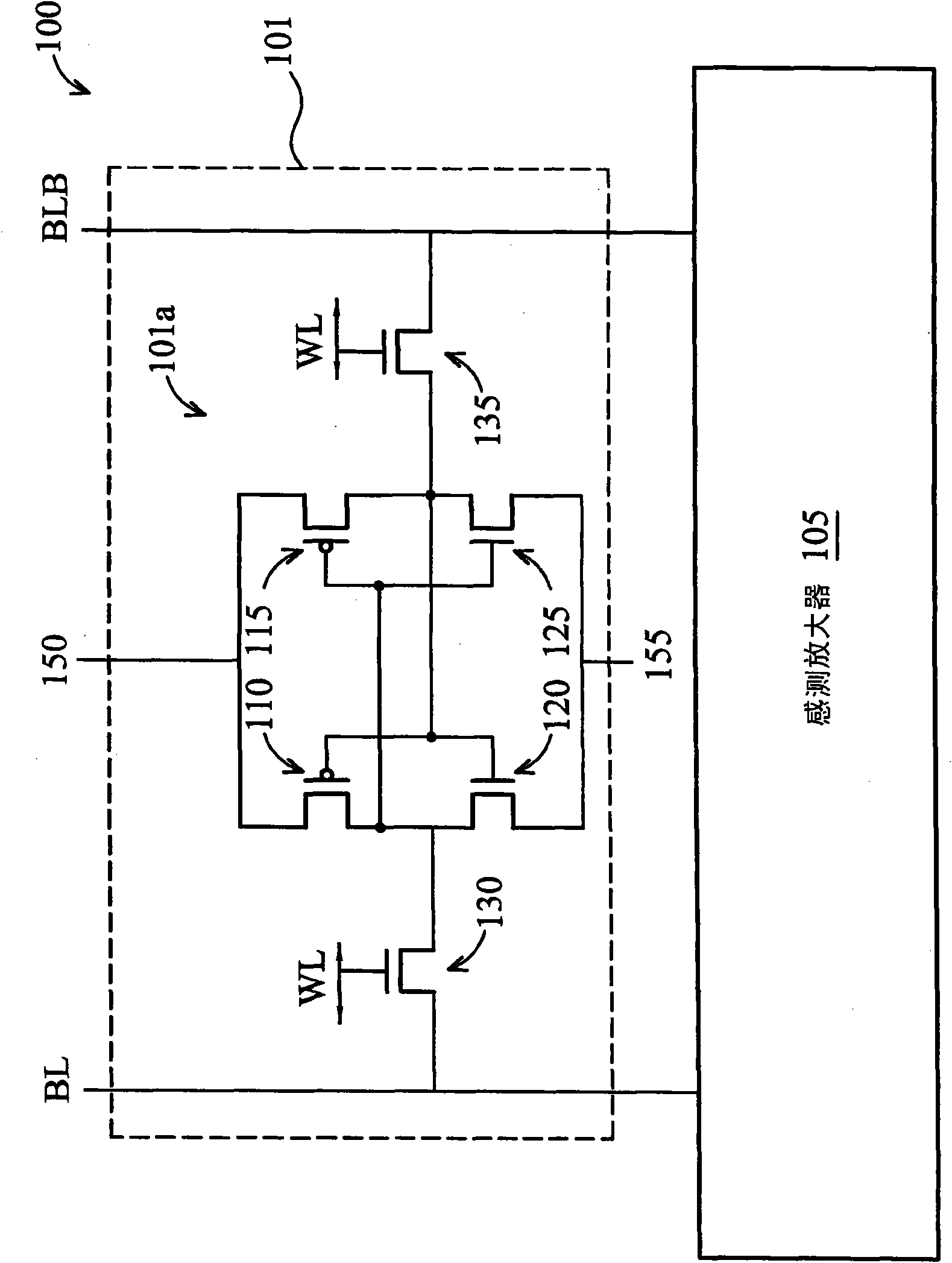
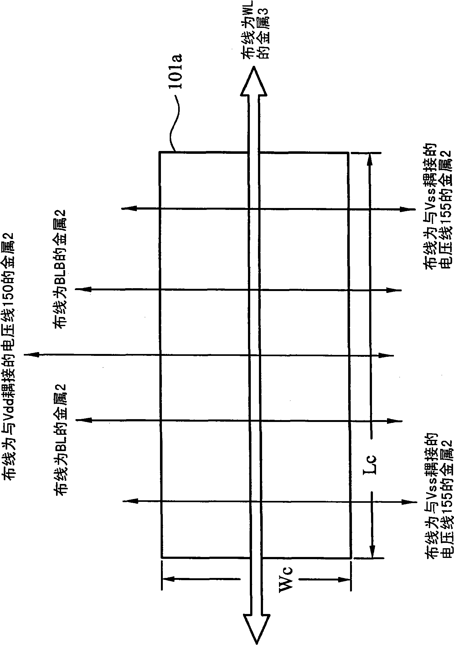
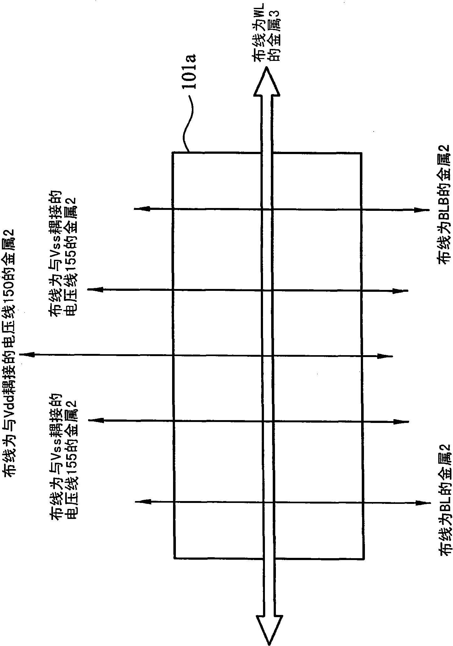
[0034] In order to make the above-mentioned objects, features and advantages of the present invention more comprehensible, preferred embodiments will be described in detail below together with the accompanying drawings.

[0035] It can be appreciated that the following disclosure provides many different embodiments or examples for implementing different features. Specific example combinations and permutations are described below to simplify the present invention. Of course this is only an example and not a limitation. For example, when describing the form of a first feature on a second feature, it may include that the first feature is in direct contact with the second feature, and it may include that an additional feature is formed between the first feature and the second feature such that The first and second features may not be in direct contact. In addition, the present invention may repeat reference numerals and / or letters in various embodiments. These repetitions are f...


PUM


Abstract

A memory circuit includes at least one memory cell for storing a datum. The memory cell is coupled with a word line, a bit line, a bit line bar, a first voltage line, and a second voltage line. The memory circuit includes a first conductive layer, a second conductive layer coupled with the first conductive layer, a third conductive layer coupled with the second conductive layer. The third conductive layer is routed for the word line and is free from including the bit line, the bit line bar, the first voltage line, and the second voltage line within the memory cell.

Description

technical field [0001] The present invention relates to semiconductor circuits, and more particularly to the wiring of memory circuits and their conductive layers. Background technique [0002] Memory circuits have been implemented in various applications. Memory circuits may include dynamic random access memory (DRAM), static random access memory (SRAM), and non-volatile memory circuits. The SRAM circuit includes a plurality of memory cells (cells). For a 6-T static memory that provides an array of memory cells, each of the memory cells contains six transistors. The 6-T SRAM memory cell is coupled to a bit line BL, an inverted bit line BLB and a word line WL. Four of the six transistors form two sets of interleaved-coupled inverters for storing data representing "0" or "1". The remaining two transistors are used as access transistors to control the access of data stored in the memory cell. [0003] The 6-T SRAM memory cell, as mentioned above, is also coupled to the po...

Claims


Application Information

Patent Timeline
Patent Type & Authority Applications(China)
IPC IPC(8): G11C11/413G11C11/41
CPCH01L27/0207H01L23/50H01L27/11H01L27/1104G11C11/412H01L2924/0002H10B10/00H10B10/12H01L2924/00G11C5/06G11C5/063G11C11/4097
Inventor 廖忠志
Owner TAIWAN SEMICON MFG CO LTD
Why Eureka
Try Eureka