
Multi-frequency scanning infrared touch device

A technology of multi-frequency scanning and infrared touch screen, which is applied in the direction of instruments, electrical digital data processing, and input/output process of data processing, etc. It can solve the problems of increasing the design and manufacturing costs of infrared touch devices, increasing the complexity of software and hardware, and hysteresis , to achieve the effect of simple software and hardware structure, easy debugging and low production cost

Inactive Publication Date: 2010-07-28
深圳新山鹰互动技术有限公司
View PDF2 Cites 22 Cited by
  • Summary
  • Abstract
  • Description
  • Claims
  • Application Information

AI Technical Summary

Problems solved by technology

Patent application 200610037391.X provides a technical solution using multiple master-slave microcontrollers. Although it can realize functions such as fast scanning and anti-interference, the disadvantage of multi-processors is that it greatly increases the complexity of the software and hardware in the entire system. degree, increasing the design and manufacturing cost of the infrared touch device
The technical solution disclosed in the patent application 200610140874.2 adopts a method of tracking the touch object to shorten the time required for detecting the touch object. It only involves the change of the internal control software of the microcontroller system, so it hardly increases the complexity and complexity of the system hardware. However, since the tracking range adopts a specific algorithm, when the touch object moves fast, or suddenly moves quickly, it is often the case that the touch object cannot be tracked and the whole area needs to be re-scanned, resulting in pauses and hysteresis

Method used


Image

  • Multi-frequency scanning infrared touch device
  • Multi-frequency scanning infrared touch device
  • Multi-frequency scanning infrared touch device

Examples


Embodiment Construction

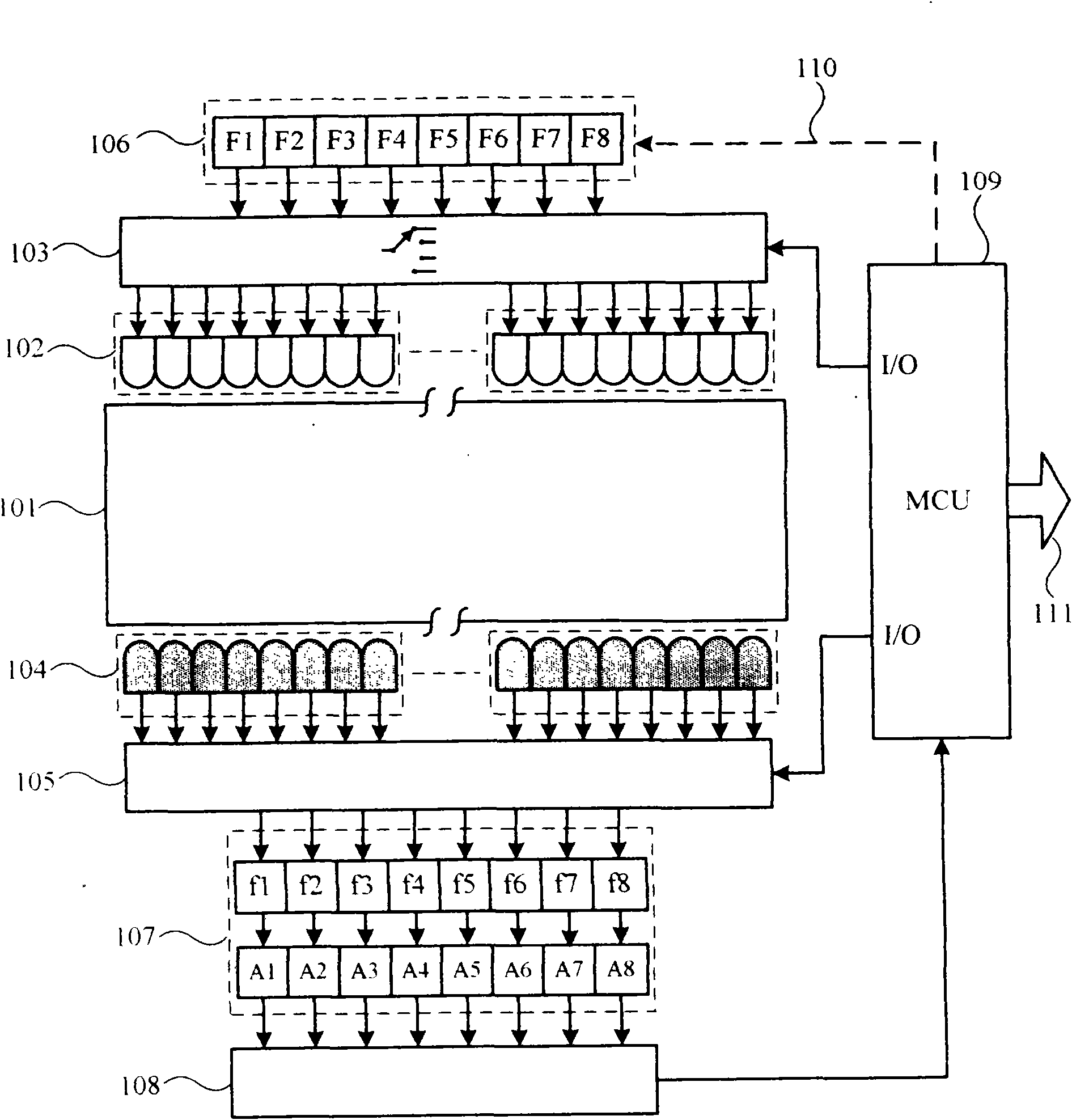
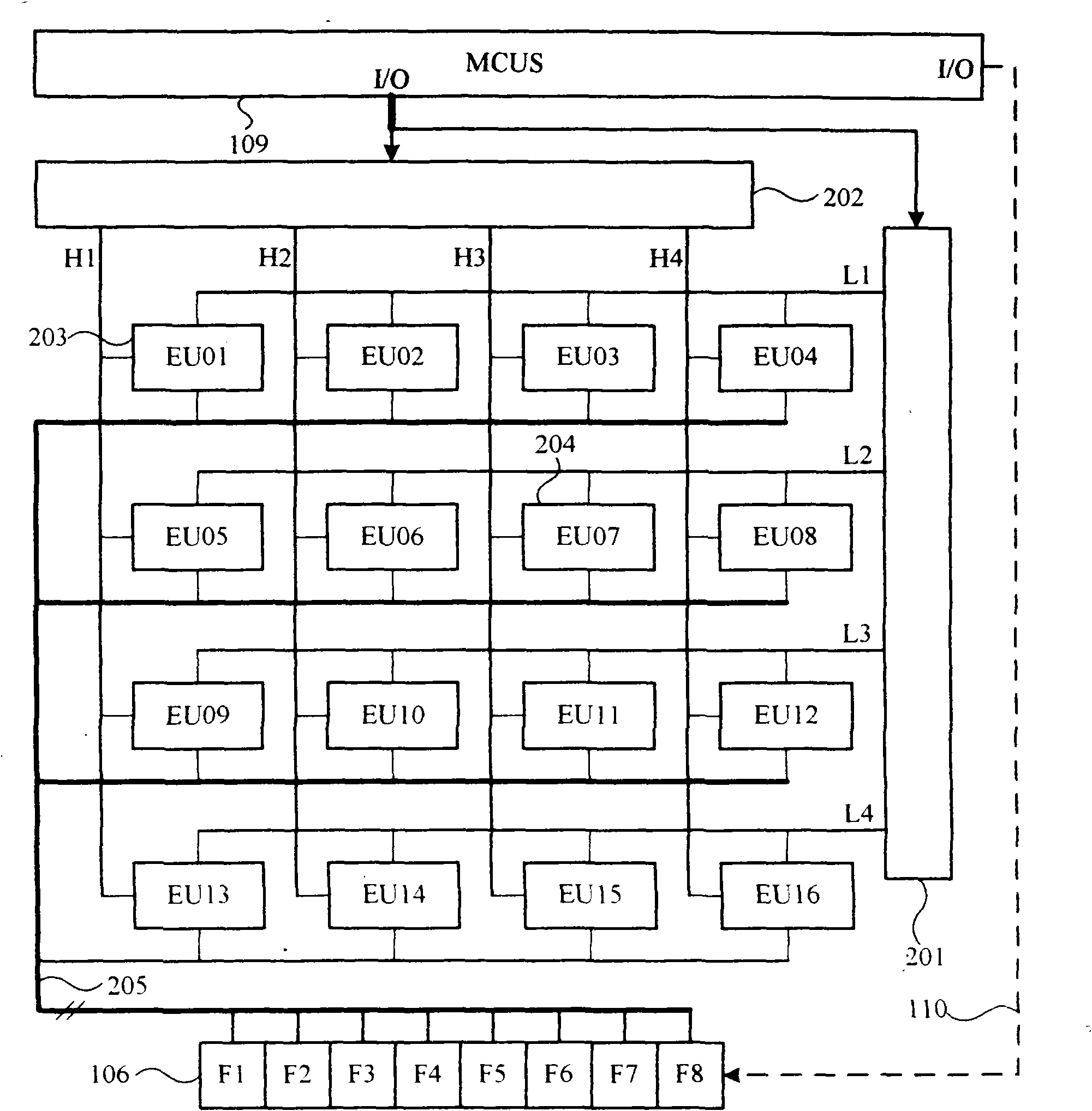
[0025] The basic embodiments of the present invention will be described below in conjunction with the accompanying drawings. Because the technical solution involved in the present invention is about the content of the circuit part for transmitting and receiving infrared signals, the specific mechanical structure of the infrared touch device (infrared touch screen) will not be given in the embodiment.

[0026] figure 1It is a schematic diagram of the overall circuit structure of the infrared touch device of the present invention. Compared with the basic structure of the existing infrared touch device, the biggest difference in this figure is that the touch device contains a carrier frequency source group 106, which contains 8 carrier frequency sources F1 to F8, and at the same time, the receiving end adds The same number of signal amplification processing circuits, and the number of frequency sources and signal amplification processing circuits is the same as the number of inf...


PUM


Abstract

The invention discloses a multi-frequency scanning infrared touch device. Infrared emitters and receiving geminate transistors are divided into a plurality of groups, each emitter in each emitter group is simultaneously driven by a carrier frequency source and a drive module of the infrared emitter; and the number of the carrier frequency sources is the same with the number of the emitters in a emitter group, but the frequencies thereof are different. The electrooptical signal output end of each detector in each detector group is connected with the output ends of the receiving tube with the same number in other detector groups, and then is connected with an amplification processing unit comprising a filter which corresponds to the output frequency of each carrier frequency source, and theprocessed result is transmitted to a microcontroller controlling the touch device for realizing the coordinate detection of a touched object. The invention has the advantages of driving multiple pairs of emitters and the receiving tube in one group simultaneously and performing scanning detection without mutual interference, thus being capable of improving scanning speed by multiple times and being suitable for infrared touch devices with a larger size.

Description

technical field [0001] The invention relates to an infrared touch device, which belongs to the technical field of computer human-computer interaction, in particular to the technical field of touch point detection and scanning for an infrared touch device. Background technique [0002] The main structure and principle of the existing infrared touch device (that is, the infrared touch screen in general sense) is to install several pairs of infrared emitting and receiving tubes on the frame, and then use the microcontroller system inside the touch device through the I / O port to Control the driving module for driving the infrared emitting tube and the gating module for gating the infrared receiving tube, drive and gating each pair of infrared emitting and receiving tubes in a certain order, and complete the vertical and horizontal scanning of the touch surface. Then by detecting which pair of emitting and receiving tubes is blocked, the position of the touch object on the displa...

Claims


Application Information

Patent Timeline
IPC IPC(8): G06F3/042
Inventor 肖衣鉴
Owner 深圳新山鹰互动技术有限公司
Features
  • Generate Ideas
  • Intellectual Property
  • Life Sciences
  • Materials
  • Tech Scout
  • Unparalleled Data Quality
  • Higher Quality Content
  • 60% Fewer Hallucinations
Learn More