Detection device of subsurface defect of optical element and method thereof

A technology for subsurface defects and optical components, applied in the direction of optical testing flaws/defects, etc., can solve the problems of measurement result error, unreliable depth and topography measurement results, etc., to avoid measurement errors, optimize grinding and polishing processes, improve The effect of processing efficiency

Inactive Publication Date: 2010-09-01
成都精密光学工程研究中心
View PDF4 Cites 40 Cited by
  • Summary
  • Abstract
  • Description
  • Claims
  • Application Information

AI Technical Summary

Problems solved by technology

In this method, the ground sample is first partially polished and etched, and then the profiler is used to measure the surface profile of the side area along a certain direction from the grinding area to the polishing area to obtain the shape of the measured area, that is, the depth Z( Height) changes with the X (horizontal) direction, and then use a microscope to observe the same area. When observing, the micr

Method used


Image

  • Detection device of subsurface defect of optical element and method thereof
  • Detection device of subsurface defect of optical element and method thereof

Examples


Embodiment Construction

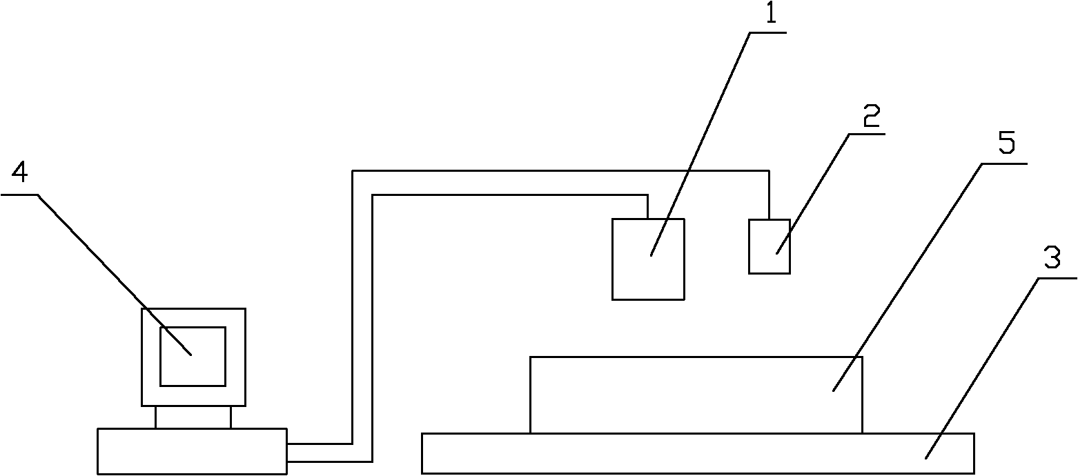
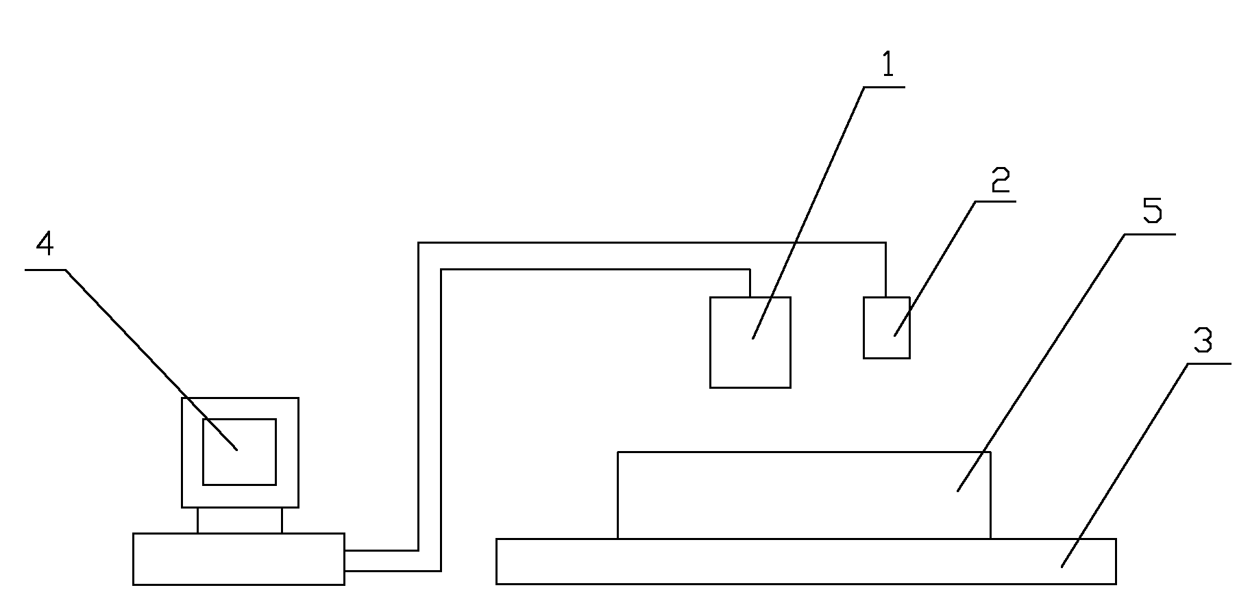
[0009] Such as figure 1 As shown, the measuring device of the present invention includes: a microscope 1, a laser displacement sensor 2, a precision displacement platform 3, and an image data processing unit 4, and the image data processing unit 4 is connected to the microscope 1 and the laser displacement sensor 2 respectively. Microscope 1 has a lens with high magnification and large numerical aperture and a lens with low magnification and wide field of view. The wide field of view lens is used for preliminary positioning of the measured area, and the high magnification lens is used for precise focusing to measure the depth of subsurface defects and observe subsurfaces defect morphology. The laser displacement sensor 2 is used to measure the movement amount of the precision displacement platform 3 in the Z direction, and the laser displacement sensor 2 has a measurement accuracy above submicron level. The precision displacement platform 3 is used to place the sample 5 and p...


PUM


Abstract

The invention provides a detection device of subsurface defect of an optical element with little measurement error and a method thereof. The detection device of the subsurface defect of the optical element comprises a microscope, a precise displacement platform and an image data processing unit connected with the microscope, wherein thethe image data processing unit is further connected with a laser displacement sensor which is used for measuring the movement amount of the precise displacement platform in the direction Z. In the invention, the optical microscope and the laser displacement sensor are adopted for measuring the subsurface detect, the subsurface defect depth and the appearances of the subsurface detect under different depths are obtained, and the observation of the appearances of the subsurface detect under different depths and the accurate depth measurement are realized, error resulting from the reposition of the traditional detection is avoided, and micron-level measurement precision is ensured. The invention is used for the detection of the subsurface defect of optical glass, and is suitable for the measurement of processing subsurface defect of ceramic, silicon, germanium and other engineering materials.

Description

technical field [0001] The invention relates to the field of optical processing and detection, in particular to a detection device and method for subsurface defects generated in the processing and grinding stages of optical elements. Background technique [0002] With the development of large-scale laser optical systems, astronomical telescopes and space telescope systems, the requirements for the processing quality of optical components are becoming more and more stringent. Over the years, studies on the causes of defects in optical components have shown that subsurface defects such as microcracks generated during the manufacturing process of optical components are important factors that cause defects in optical components. The lifetime and performance of optical components in optical systems are affected by their processing quality, especially subsurface defects. Therefore, accurate and effective measurement of the degree and depth of subsurface defects in optical compone...

Claims


Application Information

Patent Timeline
IPC IPC(8): G01N21/88
Inventor 李亚国雷向阳郑楠邓燕谢瑞清陈贤华王健许乔
Owner 成都精密光学工程研究中心
Why Eureka
Try Eureka