Method for preparing patterned sapphire substrate for extension of gallium nitride-based LED

A patterned substrate, gallium nitride-based technology, applied in electrical components, circuits, semiconductor devices, etc., can solve the problems of difficult control of the manufacturing process, limiting the quantum efficiency of light-emitting diodes, and insignificant improvement in reflectivity, and achieves the goal of preparing The method is simple and diverse, the preparation process is easy to control, and the effect of reducing the production cost

Inactive Publication Date: 2010-09-08
WUHAN XIRUI TECH
View PDF7 Cites 14 Cited by
  • Summary
  • Abstract
  • Description
  • Claims
  • Application Information

AI Technical Summary

Problems solved by technology

[0002] Gallium nitride-based light-emitting diodes commonly used in the world are mainly heteroepitaxy on a flat substrate, where the substrate can be sapphire, silicon carbide or silicon. The main disadvantages of this structure are: 1. Since there is no lattice matching GaN-based light-emitting diodes are grown on substrates such as sapphire, silicon carbide, or silicon. The difference in lattice constants causes many dislocations in the epitaxial materials. These defects limit the light-emitting diodes. 2. When light enters the substrate from the epitaxial layer, because the interface is relatively flat, the incident angle of light is relatively small, and the refractive index difference between gallium nitride and the substrate is not large, resulting in low reflectivity, and most of the light will Escape to the substrate and cannot be effectively reflected back to the epitaxial layer, which greatly reduces the light extraction efficiency of GaN-based light-emitting diodes
For example, Korean patents with publication numbers 1020080087406 and 1020060127623 make a hemispherical mask on sapphire and etch the sapphire to obtain a hemispherical pattern. Although the above method partially reduces epitaxial defects and improves light extraction efficiency, it still has the following disadvantages: Since the refractive index of sapphire is 1.8, which is similar to that of gallium nitride, when light enters the patterned substrate from the epitaxial layer, the reflectivity does not increase significantly, and the improvement of the light extraction rate of gallium nitride-based light-emitting diodes cannot reach expected result
[0004] Because the sapphire substrate is relatively hard, the production process has high requirements on equipment and technology, especially the dry etching of sapphire requires a helium cooling system and high-density plasma. Ordinary etching equipment cannot meet the requirements. Corrosion method requires the use of strong acid at high temperature, and the production process is difficult to control, resulting in low yield and increased production cost

Method used


Image

  • Method for preparing patterned sapphire substrate for extension of gallium nitride-based LED
  • Method for preparing patterned sapphire substrate for extension of gallium nitride-based LED
  • Method for preparing patterned sapphire substrate for extension of gallium nitride-based LED

Examples


Embodiment Construction

[0012] A method for preparing a gallium nitride-based LED epitaxy sapphire patterned substrate, the steps of which are:

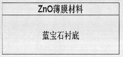
[0013] a On a 2-inch c-plane sapphire substrate, a layer of 0.6 μm ZnO film was grown by chemical vapor deposition, such as figure 1 shown;

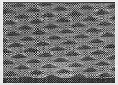
[0014] b Prepare a hemispherical mask on the ZnO film with photoresist;

[0015] c. By dry etching, the hemispherical photoresist mask pattern is transferred to the ZnO film to form hemispherical ZnO on the sapphire substrate, and the ZnO material between the hemispheres is etched clean to expose the sapphire substrate;

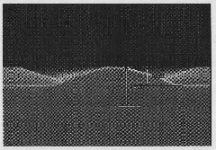
[0016] d cleans the sapphire substrate to prepare a sapphire pattern substrate such as figure 2 , 3 shown.

[0017] The bottom circle of the GaN-based light-emitting diode epitaxial substrate formed through the above steps has a diameter of 1 μm to 5 μm, a height of 0.5 μm to 3 μm, and a pattern pitch of 1 μm to 5 μm.

[0018] In the above embodiment, the pattern size of the gallium nitride-bas...


PUM

PropertyMeasurementUnit
thicknessaaaaaaaaaa
diameteraaaaaaaaaa
heightaaaaaaaaaa

Abstract

The invention discloses a method for preparing a patterned sapphire substrate for the extension of a gallium nitride-based LED, which comprises the following steps of: vapor-depositing a layer of thin film made from a low-refractive index material on the sapphire substrate by using conventional technology; preparing a mask pattern on the thin film with a photoresistor; transferring a pattern of a photosensitive resist mask onto the thin film by etching; and cleaning the substrate to remove the residual photoresistor. As threading dislocation is deflected from a vertical direction to a horizontal direction when GaN is extended and grown on the patterned substrate obtained by the method, the threading dislocation density of a GaN-based extension layer is reduced, the crystal quality of the extension layer is improved, a non-radiative recombination centre of a semiconductor luminous material is reduced, radiative recombination is enhanced and the light emitting efficiency of the LED can be improved; and the method has the advantages of easily controlled preparation process, simplicity, diversity, high rate of finished products and production cost reduction.

Description

technical field [0001] The invention relates to a light-emitting diode (LED) epitaxial substrate and a preparation method thereof, in particular to a preparation method of a gallium nitride-based LED epitaxial sapphire patterned substrate. Background technique [0002] Gallium nitride-based light-emitting diodes commonly used in the world are mainly heteroepitaxy on a flat substrate, where the substrate can be sapphire, silicon carbide or silicon. The main disadvantages of this structure are: 1. Since there is no lattice matching GaN-based light-emitting diodes are grown on substrates such as sapphire, silicon carbide, or silicon. The difference in lattice constants causes many dislocations in the epitaxial materials. These defects limit the light-emitting diodes. 2. When light enters the substrate from the epitaxial layer, because the interface is relatively flat, the incident angle of light is relatively small, and the refractive index difference between gallium nitride an...

Claims


Application Information

Patent Timeline
Patent Type & Authority Applications(China)
IPC IPC(8): H01L33/20
Inventor 陈莉姚涛陈霞周小宁
Owner WUHAN XIRUI TECH
Why Eureka
Try Eureka