Magnetic field sensor
A magnetic field sensor and substrate technology, applied in the direction of the magnitude/direction of the magnetic field, instruments, devices using electro-magnetic effects, etc., can solve the problems of low sensitivity, low linearity, incompatibility, etc., and achieve high sensitivity and high linearity Effect
- Summary
- Abstract
- Description
- Claims
- Application Information
AI Technical Summary
Problems solved by technology
Method used
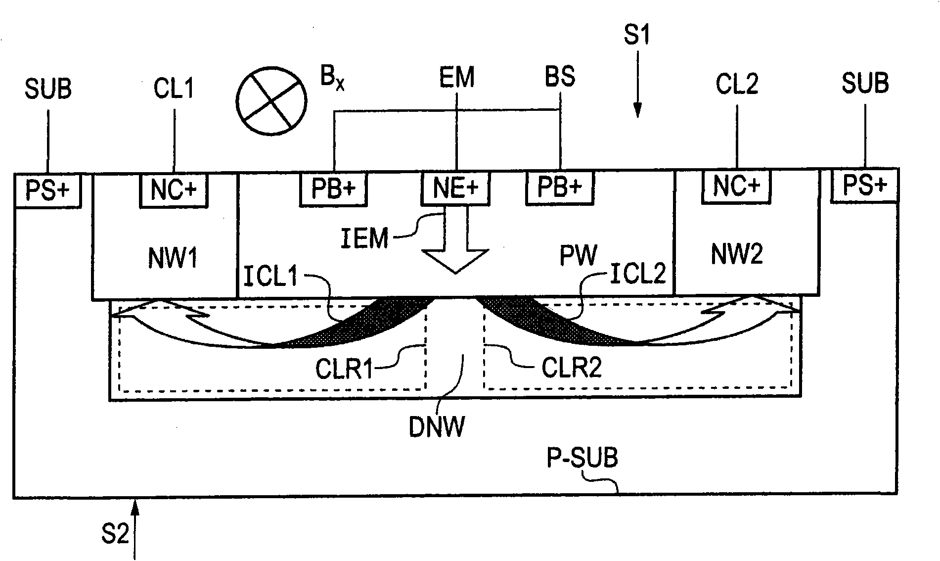
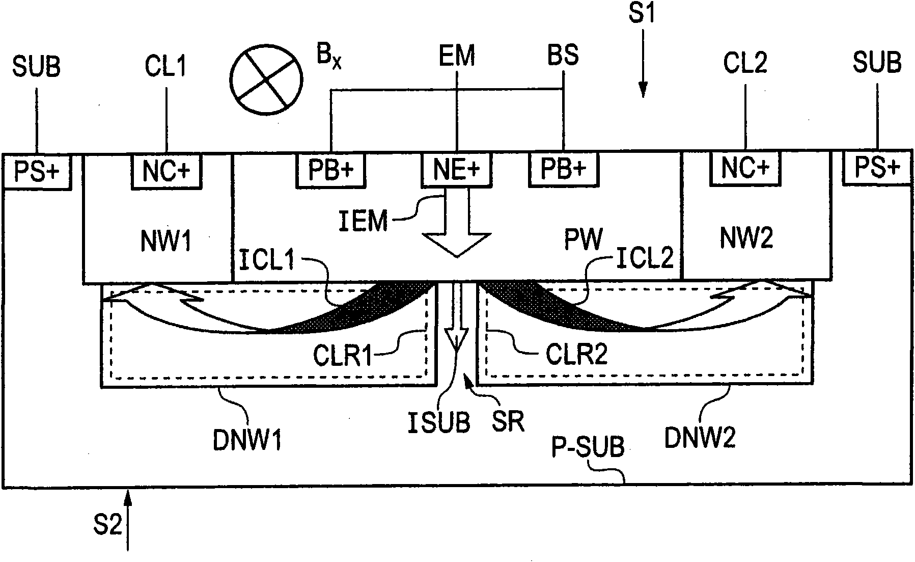
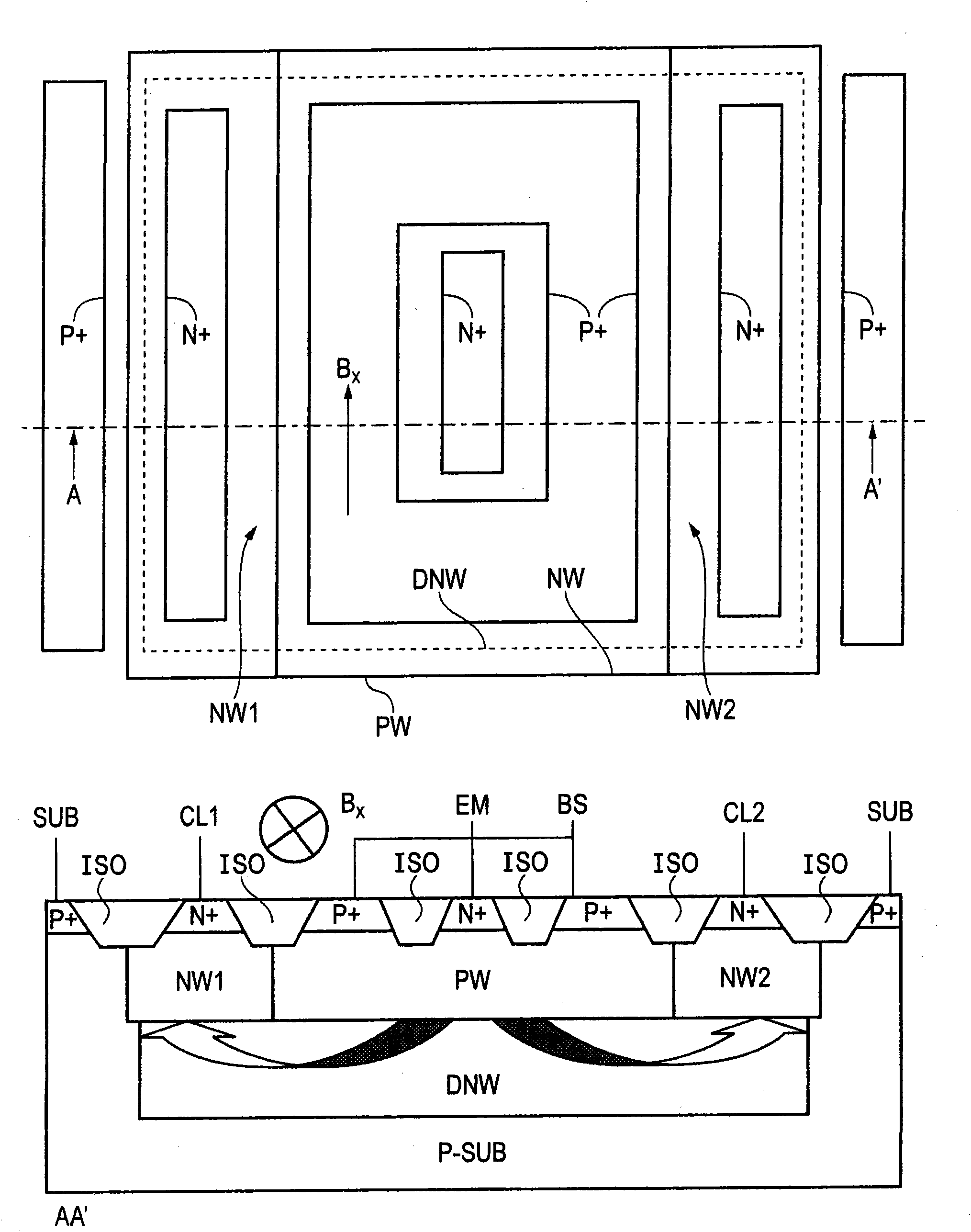
Image

Examples
Embodiment Construction
[0044] It should be noted that the above-mentioned embodiments illustrate rather than limit the invention, and that those skilled in the art will be able to design many alternative embodiments without departing from the scope of the appended claims. In the claims, any reference signs placed between parentheses shall not be construed as limiting the claim. Use of the verb "to comprise" and its conjugations does not exclude the presence of elements or steps other than those in a claim. The article "a" or "an" preceding an element does not exclude the presence of a plurality of such elements. The invention can be implemented by means of hardware comprising several distinct elements, and by a suitably programmed computer. In the device claims enumerating several means, several of these means can be implemented by one and the same piece of hardware. Importantly, the mere fact that certain measures are recited in mutually different dependent claims does not indicate that these mea...
PUM
 Abstract
Description
Claims
Application Information
 - R&D
- Intellectual Property
- Life Sciences
- Materials
- Tech Scout
- Unparalleled Data Quality
- Higher Quality Content
- 60% Fewer Hallucinations
Browse by: Latest US Patents, China's latest patents, Technical Efficacy Thesaurus, Application Domain, Technology Topic, Popular Technical Reports.
© 2025 PatSnap. All rights reserved.Legal|Privacy policy|Modern Slavery Act Transparency Statement|Sitemap|About US| Contact US: help@patsnap.com