Scalable silicon-based microdisplay driver circuit
A technology of microdisplay and driving circuit, applied in static indicators, instruments, etc., can solve problems such as reducing data transmission efficiency
- Summary
- Abstract
- Description
- Claims
- Application Information
AI Technical Summary
Problems solved by technology
Method used
Image

Examples
no. 1 example
[0036] Such as figure 1 As shown, the scalable silicon-based microdisplay driver circuit of the present invention includes a metal oxide semiconductor field effect transistor, a metal electrode and a light emitting device positioned above the metal electrode, and is characterized in that:
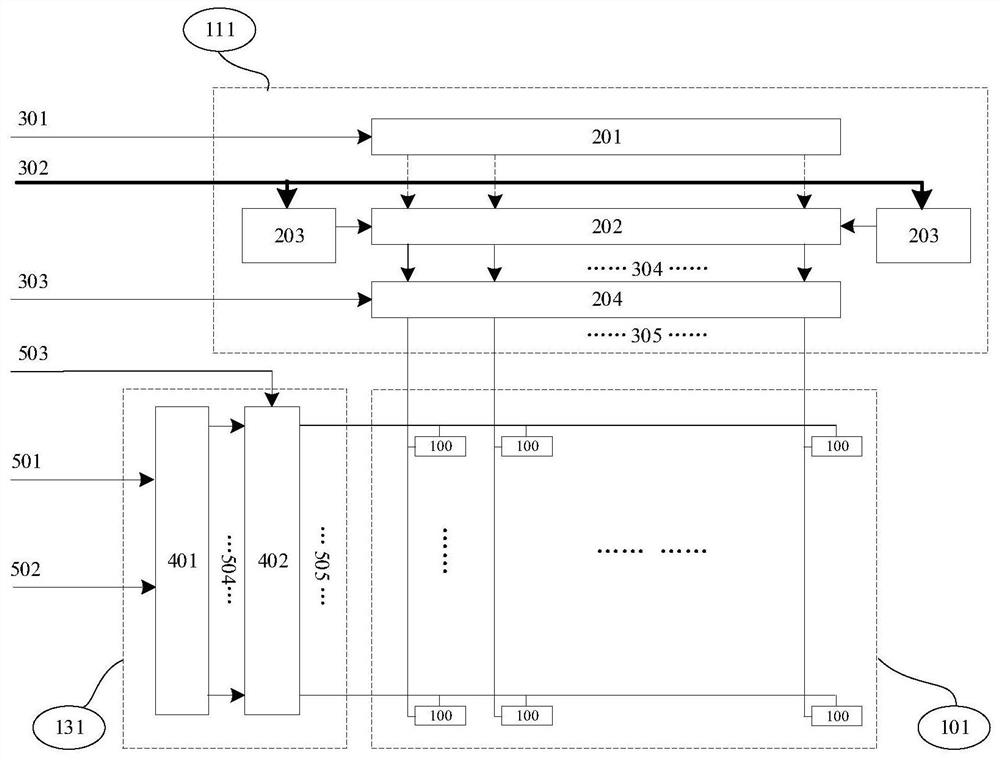
[0037] The driving circuit includes a pixel array circuit 101 , a column driving circuit 111 , and a row driving circuit 131 .
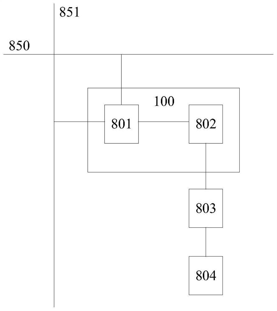
[0038] The pixel array circuit 101 includes effective M columns and N rows of pixel circuits 100 arranged in an array, and each pixel circuit 100 is as figure 2 As shown, they all include a pixel data control circuit 801 and a drive transistor 802. The pixel data control circuit 801 reads out the data on the column data 851 and generates a drive signal for the drive transistor 802 when the row selection signal 850 is valid. The driving transistor 802 is used to generate microcurrent or microvoltage required by the light emitting device 804 according to the drivi...
no. 2 example
[0042] In this embodiment, the silicon-based microdisplay driver circuit is basically the same as the first embodiment, especially in that, as Figure 5 As shown, the column drive circuit 111 includes an odd column drive circuit 112 and an even column drive circuit 113 respectively located on both sides of the drive circuit, the odd column drive circuit 112 is used to drive all odd columns, and the even column drive Circuit 113 is used to drive all even columns.
[0043] The odd-column drive circuit 112 includes an odd-column clock tree 211, an odd-column bidirectional parallel shift register 212, an odd-column offset controller 213, and an odd-column driver 214, and the even-column drive circuit 113 includes an even-column clock tree 221, An even-column bidirectional parallel shift register 222 , an even-column offset controller 223 , and an even-column driver 224 . The operation modes of the odd-column driving circuit 112 and the even-column driving circuit 113 are the same...
no. 3 example
[0046] In this embodiment, the silicon-based microdisplay driver circuit is basically the same as the first embodiment, especially in that, as Figure 6 As shown, the driving circuit 111 is divided into an upper driving circuit and a lower driving circuit: the upper driving circuit includes an upper driving circuit 114 and an upper driving circuit 132, and the upper driving circuit 114 is used to generate the upper driving circuit in the pixel array 101. The column data signal group 335 of the half pixel circuit, the upper row driver circuit 132 is used to generate the row selection signal group 525 of the upper half pixel circuit in the pixel array 101; the lower driver circuit includes the following driver circuit 115 and the lower driver circuit 133, the following driving circuit 115 is used to generate the column data signal group 345 of the lower half of the pixel circuits in the pixel array 101, and the lower row driving circuit is used to generate the row selection signa...
PUM
 Abstract
Description
Claims
Application Information
 - R&D
- Intellectual Property
- Life Sciences
- Materials
- Tech Scout
- Unparalleled Data Quality
- Higher Quality Content
- 60% Fewer Hallucinations
Browse by: Latest US Patents, China's latest patents, Technical Efficacy Thesaurus, Application Domain, Technology Topic, Popular Technical Reports.
© 2025 PatSnap. All rights reserved.Legal|Privacy policy|Modern Slavery Act Transparency Statement|Sitemap|About US| Contact US: help@patsnap.com