Multi-project wafer cutting method for improving finished product rate of chips

A multi-project, chip technology, applied in electrical components, semiconductor/solid-state device manufacturing, circuits, etc., to achieve the effect of reducing the number, taking into account cutting requirements, and reducing the area of ​​​​the mask

Inactive Publication Date: 2010-09-15
ZHEJIANG UNIV
View PDF2 Cites 13 Cited by
  • Summary
  • Abstract
  • Description
  • Claims
  • Application Information

AI Technical Summary

Problems solved by technology

However, it is obvious that the solution of repeatedly placing the same chip on a Reticle is not the most suitable for multi-project wafer dicing, and the latt

Method used


Image

  • Multi-project wafer cutting method for improving finished product rate of chips
  • Multi-project wafer cutting method for improving finished product rate of chips
  • Multi-project wafer cutting method for improving finished product rate of chips

Examples


Embodiment Construction

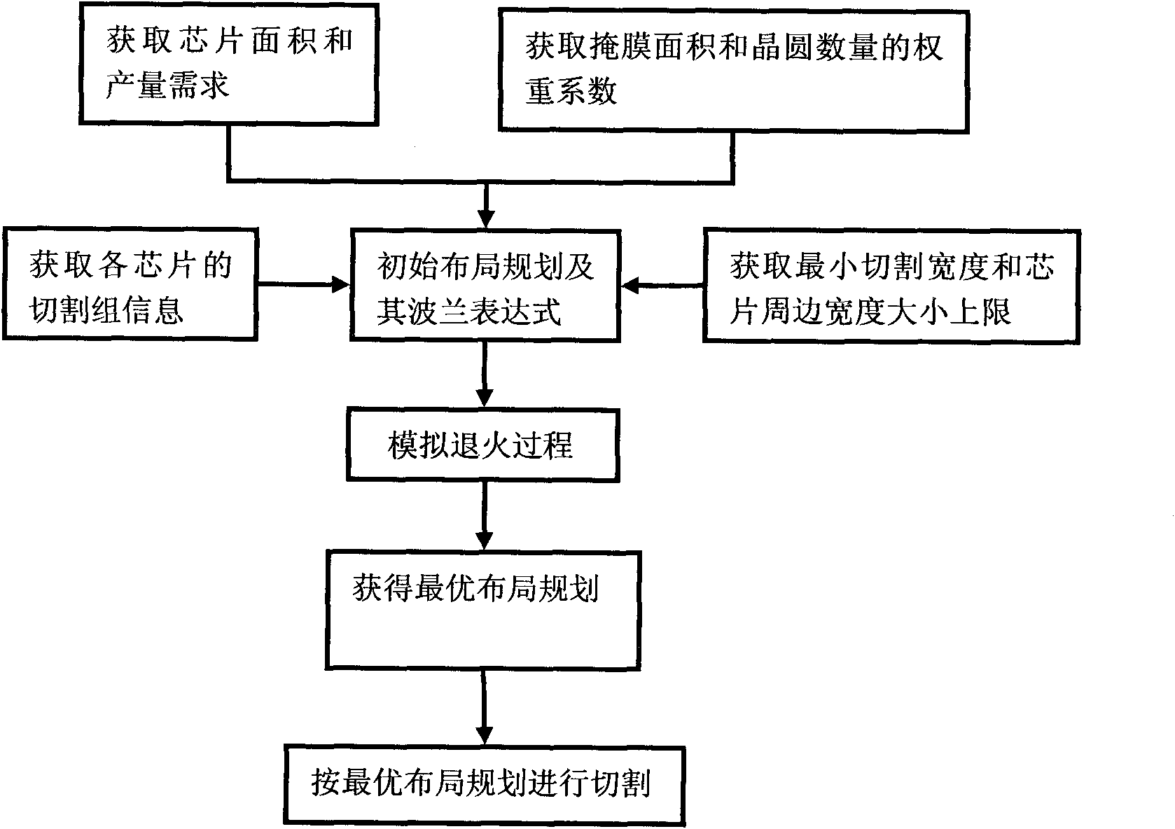
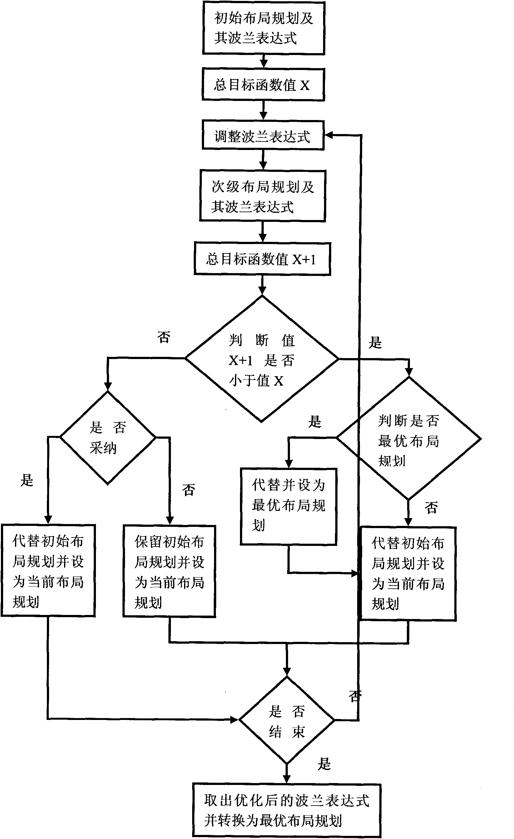
[0074] The layout planning method of the present invention will be described in detail below in conjunction with the accompanying drawings:

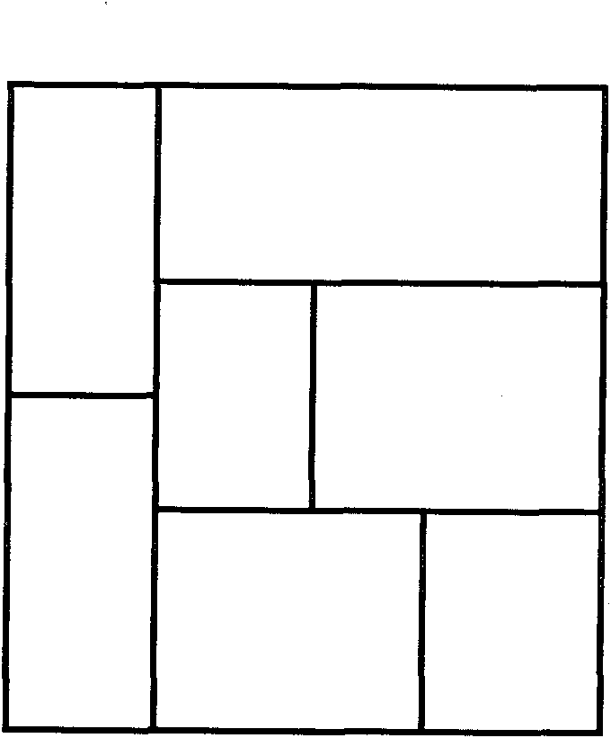
[0075] Such as figure 1 and figure 2 As shown, the flow process of the multi-item wafer cutting method for improving chip yield of the present invention is as follows:

[0076] (1) Obtain information on chip area and output requirements;

[0077] (2) Determine the priority of the chip according to the actual production demand, and attribute the chips of the same priority to the same division group; the priority of the chip is usually determined according to the actual production demand and comprehensively consider the requirements of each customer, and the production demand is large, which affects the production cost. Chips with greater impact are placed in the same priority.

[0078] (3) Obtain the information of the weight coefficient of the mask area and the number of wafers in the actual production demand; the sum of the weight ...


PUM


Abstract

The invention discloses a multi-project wafer cutting method for improving finished product rate of chips, and provides a method for cutting multi-project wafers based on an optimal layout planning acquired by quick optimal solution of a simulated annealing algorithm according to the yield demand and the cutting demand of different chips in the practical production. The method can ensure that all chips with complete functions and the same priority in the same cutting group can be simultaneously cut on the same mask plate, effectively realize the priority that the high-priority chips are not cut, furthest reduce the loss of the finished product rate of the chips caused by wafer cutting factors, meanwhile reduce the number of the wafers required for production, and reduce the production cost.

Description

technical field [0001] The invention relates to a wafer cutting method, in particular to a multi-item wafer cutting method which improves chip yield. Background technique [0002] Multi Project Wafer (Multi Project Wafer, referred to as MPW), is to put a variety of integrated circuit designs with the same process on the same mask (Reticle / Mask, also called a mask, a wafer contains multiple identical After the manufacturing is completed, dozens of chip samples can be obtained for each design project, which is enough for experiments and tests in the prototype (Prototype) design stage. The manufacturing cost is shared by all the projects participating in the multi-project wafer according to their respective chip areas, and the cost is only 5%-10% of the cost of prototype manufacturing for a single project, which greatly reduces product development risks. The threshold for cultivating integrated circuit design talents and the threshold for small and medium integrated circuit de...

Claims


Application Information

Patent Timeline
IPC IPC(8): H01L21/78H01L21/00
Inventor 张波叶翼郑勇军史峥严晓浪
Owner ZHEJIANG UNIV
Why Eureka
Try Eureka