Half-bridge drive circuit chip

A circuit chip and half-bridge drive technology, which is applied in the direction of circuits, electrical components, and electric solid-state devices, can solve the problems of large space occupation, long distance, and high cost, and achieve the effects of small space occupation, reduced production costs, and compact chips

Active Publication Date: 2010-09-15
NINGBO SEMICON INT CORP
View PDF6 Cites 15 Cited by
  • Summary
  • Abstract
  • Description
  • Claims
  • Application Information

AI Technical Summary

Problems solved by technology

[0003] In existing applications, the drive control circuit is usually separately packaged into one chip, and the two power devices used in the half-bridge drive circuit are also separately packaged into two chips. In this way, it is generally necessary to use three The package body not only has a high cost, but also takes up a lot of space. At the same time, due to the long distance between the chip packaged with the drive control circuit and the chip packaged with the power device and the distance between the two chips packaged with the power device The distance is also relatively long, so the connection between the drive control circuit and the power device and the connection between the two power devices will be longer, and the longer connection will introduce a lot of parasitic parameters

Method used


Image

  • Half-bridge drive circuit chip
  • Half-bridge drive circuit chip
  • Half-bridge drive circuit chip

Examples


Embodiment 1

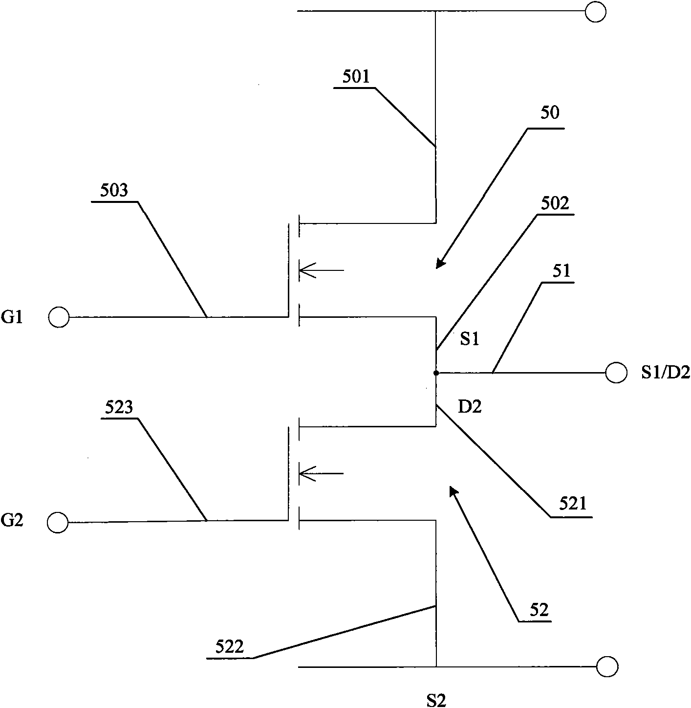
[0018] Such as image 3 As shown, a kind of half-bridge driving circuit chip that the present invention proposes, it comprises the lead frame 9 of DIP-8 (in-line eight-pin integration), and lead frame 9 has a packaging surface 91, is provided with eight mutually on the packaging surface 91. Isolated and insulated pins are the 1st pin, the 2nd pin, the 3rd pin, the 4th pin, the 5th pin, the 6th pin, the 7th pin and the 8th pin, package There are also three base islands 21, 22, 23 which are isolated and insulated from each other on the surface 91. The three base islands 21, 22, 23 are not connected to the eight pins, and each of the three base islands 21, 22, 23 has a One connecting pin, the base island 21 has a connecting pin 211, the base island 22 has a connecting pin 221, the base island 23 has a connecting pin 231, the three connecting pins 211, 221, 231 are independent of each other, and the connecting pin 211 is connected to the sixth pin , the connecting pin 221 is conn...

Embodiment 2

[0023] Such as Figure 4 As shown, in this embodiment, a SOIC-14 (Small Outline Integrated Circuit Package, Small Outline Integrated Circuit Package) lead frame 9 is used, and fourteen mutually isolated and insulated leads are arranged on the package surface 91 of the lead frame 9. The pins are the 1st pin, the 2nd pin, the 3rd pin, the 4th pin, the 5th pin, the 6th pin, the 7th pin, the 8th pin, the 9th pin, the 8th pin The 10th pin, the 11th pin, the 12th pin, the 13th pin, and the 14th pin, and three base islands 21, 22, 23 that are isolated and insulated from each other are arranged on the package surface 11, and the three base islands 21 . The six connecting pins 215, 216, 225, 226, 235, 236 are independent of each other, the connecting pin 215 is connected with the sixth pin, the connecting pin 216 is connected with the eleventh pin, and the sixth pin and the eleventh pin are connected through The base islands 21 are electrically connected to each other, the connecting...


PUM


Abstract

The invention discloses a half-bridge drive circuit chip comprising a lead frame, wherein three paddles mutually separated and insulated are arranged on an encapsulation face of the lead frame, each paddle is provided with at least one connecting pin, a drive control circuit module, a first power device and a second power device are respectively arranged on the three paddles and are mutually connected through metal leads, and the chip is formed by encapsulating the drive control circuit module, the first power device and the second power device by an encapsulation body. Compared with the three chips which are formed by respectively independently encapsulating the drive control circuit module and the two power devices, the chip is more compact; only one encapsulation body is adopted, therefore, the production cost is greatly reduced; and the distance of connection among components in the chip is smaller than that of connection among three independent chips, therefore, parasitic parameters are greatly reduced.

Description

technical field [0001] The invention relates to a package structure of a semiconductor chip, in particular to a half-bridge driving circuit chip. Background technique [0002] The half-bridge drive circuit is a common application circuit in switching power supplies, especially in the application of products such as electronic ballasts. figure 1 A schematic diagram of a typical half-bridge drive circuit is given, which includes a first power device 50 and a second power device 52, the first power device 50 is used to drive the tube on the high-voltage side, and the second power device 52 is used to drive the tube on the low-voltage side , the current input terminal 501 of the first power device 50 is connected to the high voltage terminal, the current output terminal 502 of the first power device 50 is connected to the current input terminal 521 of the second power device 52, and the current output terminal of the second power device 52 522 is connected to the power supply g...

Claims


Application Information

Patent Timeline
Patent Type & Authority Applications(China)
IPC IPC(8): H01L25/16H01L23/495H01L23/52
CPCH01L2224/48257H01L2224/48137H01L2224/49171H01L2224/49113H01L2224/48247H01L2924/1301H01L2924/1305H01L2924/13055H01L2924/13091H01L2924/00
Inventor 滕谋艳潘建立吴小晔
Owner NINGBO SEMICON INT CORP
Why Eureka
Try Eureka