Etch tank adopted in process of packaging and manufacturing TSV (Through Silicon Via) wafer and preparation process

A process method and corrosion tank technology, applied in semiconductor/solid-state device manufacturing, electrical components, circuits, etc., can solve the problems of reduced contact area, inability to realize wafer electroplating process, etc., achieve thin thickness, increase yield, The effect of simple process

Inactive Publication Date: 2010-09-22
SHANGHAI INST OF MICROSYSTEM & INFORMATION TECH CHINESE ACAD OF SCI
View PDF8 Cites 12 Cited by
  • Summary
  • Abstract
  • Description
  • Claims
  • Application Information

AI Technical Summary

Problems solved by technology

However, BCB has fluidity because it is in a molten state during the bonding process. Under the action of bonding pressure, BCB extends to the surroundings, resulting in a larger size of BCB after bonding. Since the TSV pore size is extremely small, the extended BCB It is easy to reduce or even isolate the contact area between the through hole of the TSV wafer and the metal seed layer supporting the wafer, resulting in the inability to realize the subsequent electroplating process of the wafer TSV, resulting in the failure of the TSV wafer manufacturing

Method used


Image

  • Etch tank adopted in process of packaging and manufacturing TSV (Through Silicon Via) wafer and preparation process
  • Etch tank adopted in process of packaging and manufacturing TSV (Through Silicon Via) wafer and preparation process
  • Etch tank adopted in process of packaging and manufacturing TSV (Through Silicon Via) wafer and preparation process

Examples


Embodiment Construction

[0015] In order to fully demonstrate the advantages and positive effects of the present invention, the present invention will be further described below in conjunction with the accompanying drawings and embodiments.

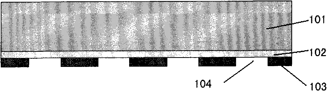
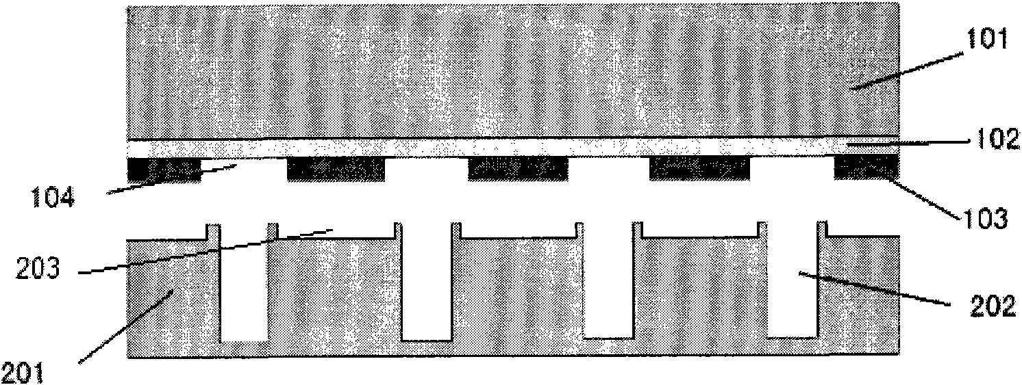
[0016] exist figure 1 In this method, a layer of Au layer 102 with strong oxidation resistance is sputtered on one side of the supporting wafer 101 with a thickness of about 100-200 nm. The role of this metal layer is to provide a seed layer for TSV electroplating Cu. Then a layer of BCB 103 is coated on the metal layer 102, and the thickness of the BCB is about 2-4 μm. The BCB is shaped by photolithography, so that the BCB that will be bonded to the TSV position 104 is removed.

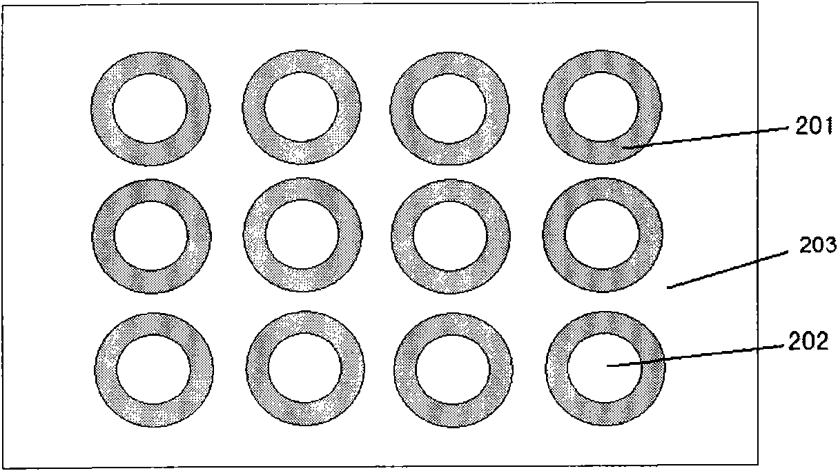
[0017] exist figure 2 Among them, using photoresist as a mask, DRIE is used to etch the etching groove 203 on the front side of the TSV wafer 201, the groove wall has a vertical feature, the depth of the etching groove is 2-3 μm, and the surface area is 1.2-1.3 times that of the BCB...


PUM


Abstract

The invention relates to an etch tank adopted in the process of packaging and manufacturing a TSV (Through Silicon Via) wafer and a preparation process. The etch tank is characterized in that the wall of the etch tank is vertical, the surface area of the etch tank is 1.2-1.3 times that of BCB (Benzocyclobutene) coated on photoetching, the depth of the vertical tank wall of the etch tank is slightly less than the thickness of the coated BCB, and the BCB is coated on a naked supporting wafer. The etch tank is made of the TSV wafer. The TSV packaging and manufacturing process comprises the following steps of: sputtering a metal layer on the naked supporting wafer, and then etching after coating a layer of BCB; etching the etch tank on the front face of the TSV wafer by using DRIE (Deep Reactive Ion Etching), and then etching a TSV array by using the DRIE, wherein the etch tank corresponds to the BCB photoetched on the supporting wafer; and bonding one face of the supporting wafer with the BCB and the front face of the TSV wafer after being aligned, and blocking the fused BCB in an extension process by using the etch tank. The structure has the function of controlling the bonding size of the BCB.

Description

technical field [0001] The present invention relates to the etch tank used in the process of encapsulating and manufacturing the wafer TSV and the corresponding process method. More precisely, the present invention is a kind of high-reliability wafer produced by using the support wafer and BCB low-temperature bonding by means of the etch tank structure. A circular TSV belongs to the technical field of wafer-level TSV three-dimensional interconnect packaging. Background technique [0002] In order to meet the needs of the development of very large scale integration (VLSI), the novel TSV (ThroughSilicon Via, Through Silicon Via) three-dimensional packaging technology came into being. It uses the smallest size and lightest weight to combine chips with different performances and multiple This technology is integrated into a single package, which is the latest packaging interconnection technology that realizes the interconnection between chips by creating vertical electrical cond...

Claims


Application Information

Patent Timeline
Patent Type & Authority Applications(China)
IPC IPC(8): H01L21/302H01L21/60
Inventor 陈骁罗乐徐高卫袁媛
Owner SHANGHAI INST OF MICROSYSTEM & INFORMATION TECH CHINESE ACAD OF SCI
Why Eureka
Try Eureka