Wide-input voltage range zero-leakage current input pull-up circuit

A technology with voltage range and large input, applied in the field of microelectronics, it can solve the problems of limited speed and difficult control of resistance, and achieve the effect of easy control.

Active Publication Date: 2010-09-22
SHANGHAI MOUNTAIN VIEW SILICON
View PDF3 Cites 12 Cited by
  • Summary
  • Abstract
  • Description
  • Claims
  • Application Information

AI Technical Summary

Problems solved by technology

However, this method cannot completely solve this problem, because although the threshold of the NativeNMOS tube is small, it is not 0
At the same time, this method brings the same problems such as difficult control of the resistance value and limited speed.

Method used


Image

  • Wide-input voltage range zero-leakage current input pull-up circuit
  • Wide-input voltage range zero-leakage current input pull-up circuit
  • Wide-input voltage range zero-leakage current input pull-up circuit

Examples


Embodiment Construction

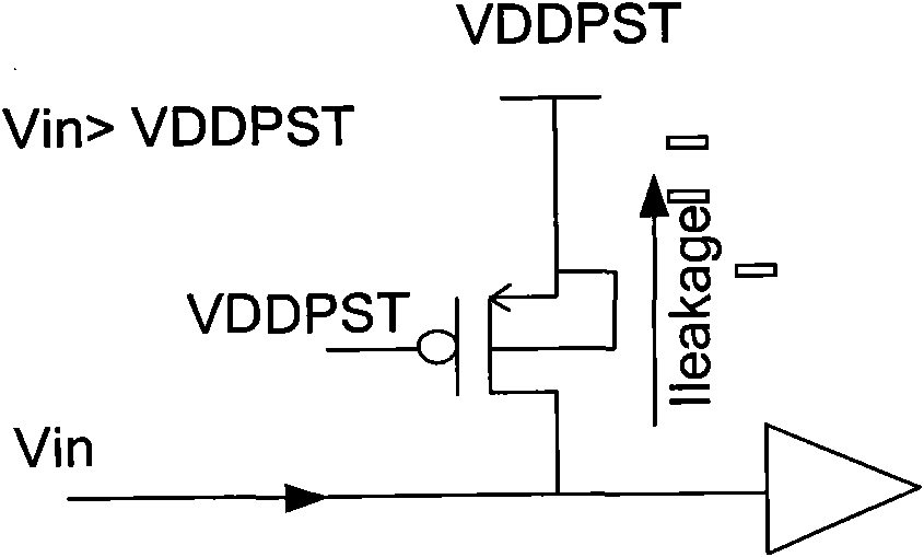
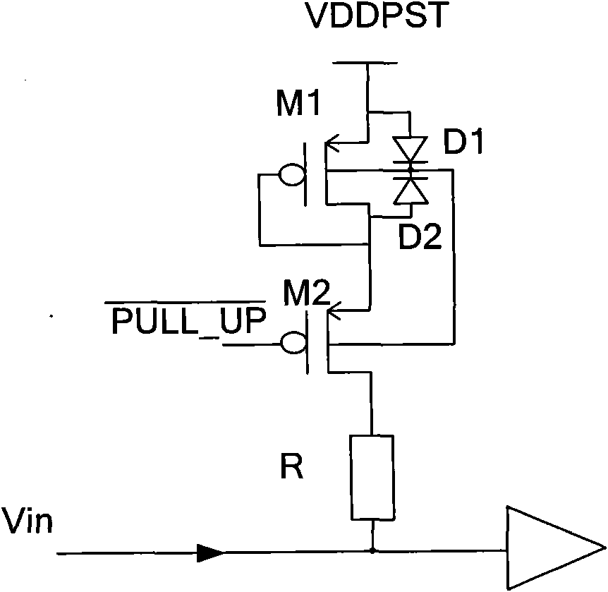
[0022] like image 3 In the shown input pull-up circuit with a large input voltage range and zero leakage current, the switch MOS transistor M2 and the reverse cut-off MOS transistor M1 are depleted PMOS transistors, and the drain of M2 is connected to the chip input signal Vin through a resistor R. The source of M2, the drain of M1 and the gate of M1 are connected.

[0023] The substrate electrode of M1 is respectively connected to the source and drain of M1 through two diodes (first anti-leakage diode D1 and second anti-leakage diode D2). The function of M1 is to play a reverse cut-off function. In this way, it can be guaranteed that when M1 is used as a diode, no matter which point of the source and drain is higher, its function is normal and there is no leakage. The substrate electrode of M2 is also connected to the substrate of M1, which also ensures that M2 has no substrate leakage current in each case.

[0024] The drain of M1 is connected to the highest input potenti...


PUM


Abstract

The invention relates to a wide-input voltage range zero-leakage current input pull-up circuit belonging to the field of microelectronics. The prior art has the problems of leakage current, froward resistance value and the like. The current output electrode of a switch MOS (Metal Oxide Semiconductor) tube of the input pull-up circuit connected with the signal input level of a chip by a controllable resistance value element; the grid electrode of the switch MOS tube is a pull-up signal input end; the current input electrode of the switch MOS tube is connected with the highest input level of the chip by a reverse cut-off circuit; and when the signal input level of the chip is higher than the highest input level, the reverse cut-off circuit is cut off. Pulling up is realized by adopting a method for dynamically changing and pulling up the MOS tube substrate to be offset and additionally arranging a diode, meanwhile, the leakage current is avoided when the input level is higher than the highest voltage of the chip.

Description

technical field [0001] The invention belongs to the field of microelectronics, in particular to a zero-leakage current input pull-up circuit with a large input voltage range. Background technique [0002] The pins of some chips must be kept at a high potential when they are suspended in order to ensure the normal operation of the internal circuits of the chip. This purpose is usually achieved by using a special input pull-up circuit. [0003] Existing input pull-up circuits such as figure 1 As shown, the source and drain of the MOS transistor are respectively connected to the input signal and the highest input potential VDDPST of the chip, and the substrate of the MOS transistor is connected to the source. When the pins of the chip are suspended, that is, there is no input signal, the MOS tube is turned on, so that the pins are kept at a high potential. When there is an input signal on the pin, the gate of the MOS is connected to the highest potential of the chip to turn o...

Claims


Application Information

Patent Timeline
Patent Type & Authority Applications(China)
IPC IPC(8): H01L23/58H01L23/48
Inventor 许刚
Owner SHANGHAI MOUNTAIN VIEW SILICON
Why Eureka
Try Eureka