Semiconductor device and manufacturing method thereof

一种制造方法、半导体的技术,应用在半导体/固态器件制造、半导体器件、半导体/固态器件零部件等方向,能够解决很难均匀分散软磁性体粉末、涡流损失效果变差、电路短路等问题,达到低价格、降低涡流损失、均匀涡流损失的效果

Inactive Publication Date: 2010-09-29
TERAMIKROS INC
View PDF3 Cites 3 Cited by
  • Summary
  • Abstract
  • Description
  • Claims
  • Application Information

AI Technical Summary

Problems solved by technology

[0007] However, in the above-mentioned semiconductor device, since the magnetic film is formed by mixing soft magnetic powder, which is a relatively expensive material, into a thermosetting resin made of polyimide resin or the like, the price becomes relatively low. high
In addition, it is difficult to uniformly disperse the soft magnetic powder in the thermosetting resin
Here, if there is a place where the soft magnetic powder is dispersed too densely, there is a danger of a short circuit.
On the other hand, if the soft magnetic powder is dispersed too loosely, the effect of reducing eddy current loss will be reduced.

Method used


Image

  • Semiconductor device and manufacturing method thereof
  • Semiconductor device and manufacturing method thereof
  • Semiconductor device and manufacturing method thereof

Examples


no. 1 approach

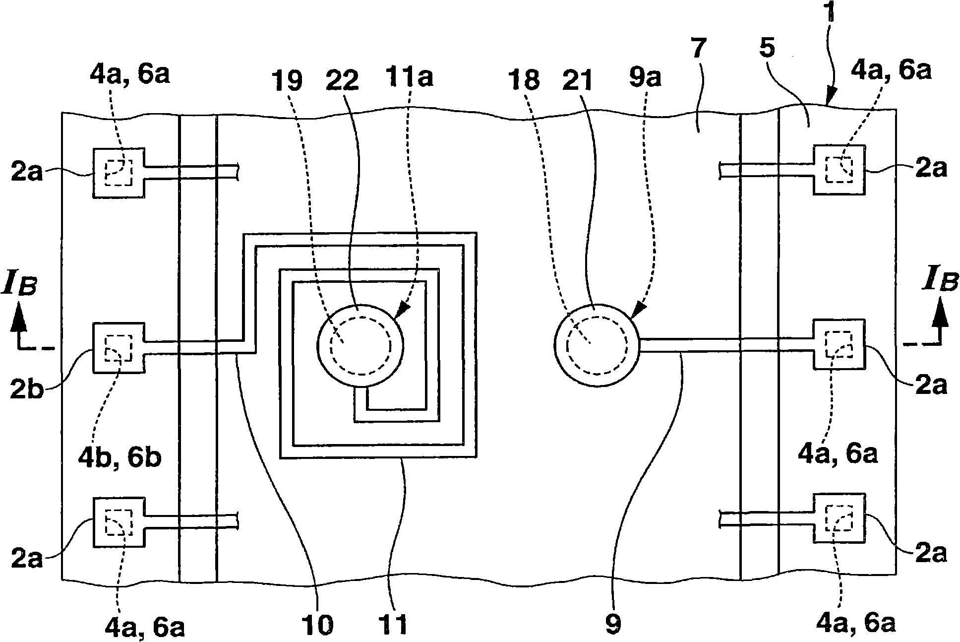
[0035] Figure 1A It is a plan view showing main parts of the semiconductor device according to the first embodiment of the present invention (excluding Figure 1B The state behind the sealing film in).

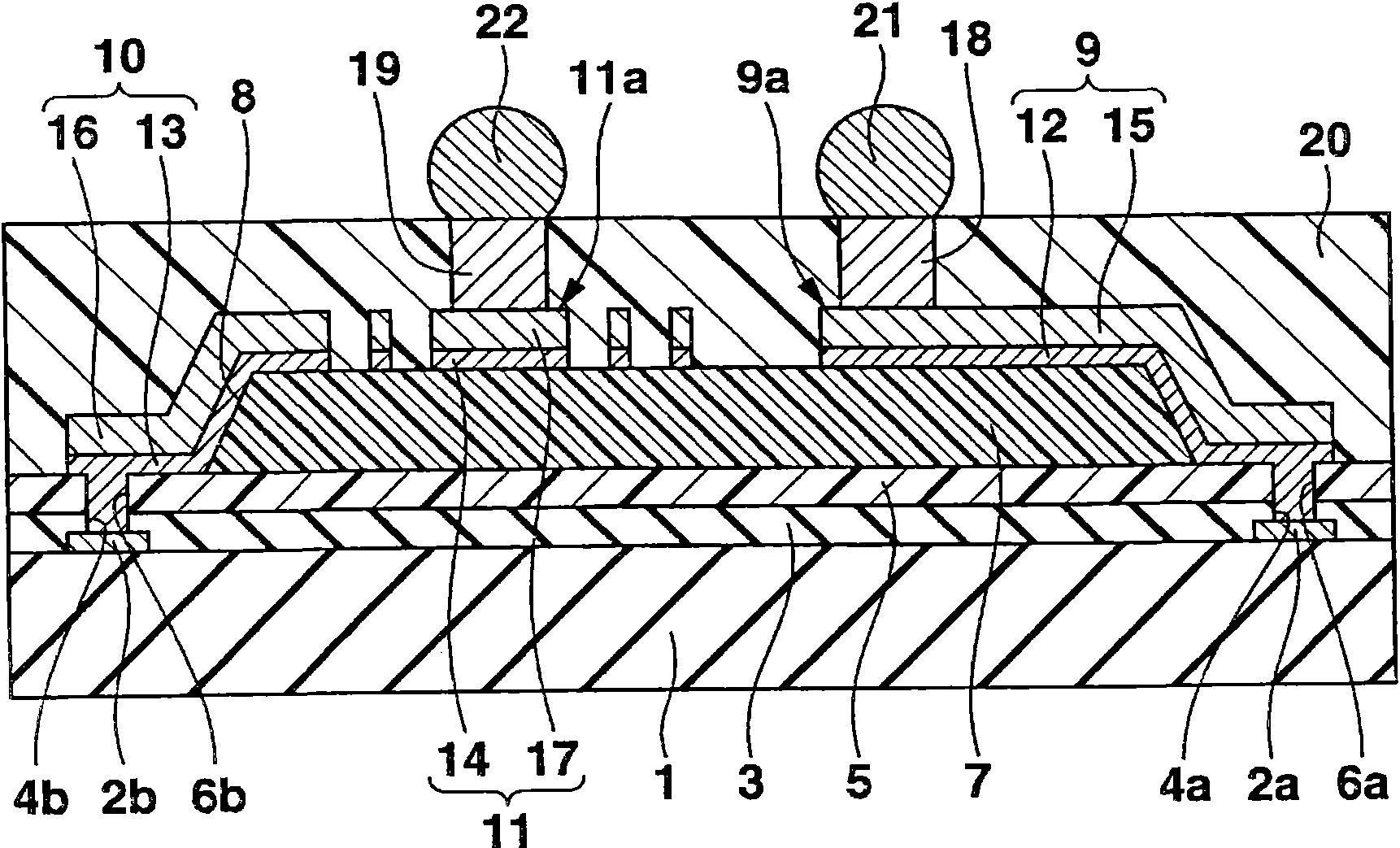
[0036] Figure 1B is along Figure 1A Sectional view of the B-B line.

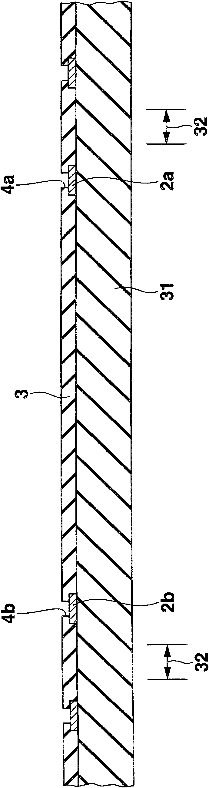
[0037] This semiconductor device has a planar square silicon substrate (semiconductor substrate) 1 generally called a CSP. On the upper surface of the silicon substrate 1, elements for forming an integrated circuit with predetermined functions, such as circuit elements (not shown) such as transistors, diodes, resistors, and capacitors, are formed. A plurality of connection pads 2a, 2b constituted by etc., and the plurality of connection pads 2a, 2b are connected to the integrated circuit. In this case, the connection pad indicated by reference numeral 2b is a member connected to the outer end of the spiral-shaped thin film sensor element 11 described later.

[0038] A passivation film 3 made of silico...

no. 2 approach

[0065] Figure 13A is a plan view of the main part of the semiconductor device according to the second embodiment of the present invention (excluding Figure 13B The state behind the sealing film in).

[0066] Figure 13B It is a cross-sectional view along line B-B.

[0067] In this semiconductor device, withFigure 1A , 1B The big difference of the shown semiconductor device is that not only the outer end of the spiral-shaped thin film sensing element 11, but also the inner end is connected to the integrated circuit (not shown) formed on the upper surface of the silicon substrate 1. ) connection pads are connected.

[0068] That is, the connection pads indicated by reference numerals 2b and 2c are connected to the inner end and the outer end of the spiral-shaped thin film induction element 13, and Figure 13A are arranged adjacently. A passivation film 3 is provided on the upper surface of the silicon substrate 1 except the central portions of the connection pads 2a, 2b,...


PUM


Abstract

The invention provides a semiconductor device and a manufacturing method thereof. The upper surface of a silicon substrate (1) is provided with a plurality of circuit elements which form an integrated circuit, wherein a passive film (3) and a first protecting film (3) are arranged thereon; the periphery of the upper surface of the silicon substrate (1) is provided with a plurality of connecting pads (2a, 2b) connected to the integrated circuit; the upper surface of the first protecting film (3), except the periphery, is provided with a second protecting film (7); and the upper surface of the second protecting film (7) is provided with a spiral film sensing element (11). The sum thickness of the first and second protecting films (5, 7) is rather thick, therefore decreasing the vortex loss of the spiral film sensing element (11) caused by generating vortex in the silicon substrate (1).

Description

[0001] Cross References to Related Applications [0002] This application is based on and claims priority from Japanese Patent Application No. 2009-075277 filed on March 25, 2009, which is incorporated herein by reference in its entirety including the specification, claims, drawings, and abstract. technical field [0003] The present invention relates to a semiconductor device and its manufacturing method. Background technique [0004] A conventional semiconductor device is known to have a spiral-shaped thin-film sensor element called a CSP (chip size package: chip size package). For example, Japanese Patent Laid-Open Publication No. 2008-210828 discloses the following semiconductor device. This semiconductor device includes a semiconductor substrate. An insulating film is provided on the upper surface of the semiconductor substrate. A plurality of wires and a spiral-shaped thin film sensor element are provided on the upper surface of the insulating film. A columnar elec...

Claims


Application Information

Patent Timeline
Patent Type & Authority Applications(China)
IPC IPC(8): H01L23/31H01L23/29H01L21/56
CPCH01L24/94H01L2924/01002H01L2224/0236H01L24/13H01L23/5227H01L2924/14H01L24/11H01L2924/01029H01L2224/024H01L2924/01078H01L2924/19041H01L2924/01013H01L2224/94H01L23/3114H01L2224/11H01L2224/03
Inventor 三原一郎
Owner TERAMIKROS INC
Why Eureka
Try Eureka