Method for growing InGaP/GaAs/Ge three-junction solar cell on silicon substrate

A technology for solar cells and silicon substrates, applied in circuits, electrical components, sustainable manufacturing/processing, etc., can solve problems such as surface topography fluctuations, lower solar cell efficiency, and increased dislocations, and achieve a wide growth process window, The effect of strong controllability and repeatability of the growth process

Inactive Publication Date: 2010-10-13
HUAZHONG UNIV OF SCI & TECH
View PDF2 Cites 20 Cited by
  • Summary
  • Abstract
  • Description
  • Claims
  • Application Information

AI Technical Summary

Problems solved by technology

However, it is not easy to epitaxially grow InGaP / GaAs / Ge triple-junction solar cells on Si substrates, because there is a 4% lattice mismatch between Si and Ge, if the Ge layer is grown directly on the Si substrate Above, a 4% lattice mismatch will trigger the S-K growth mode, that is, Ge will grow in a layered manner at the beginning, but as the thickness increases, the accumulated stress will trigger the island growth mode, and the island growth mode will trigger High-density threading dislocations, which will run through the entire InGaP / GaAs / Ge triple-junction solar cell film to the surface
Since dislocations are very efficient photo-generated carrier annihilation centers, they can seriously reduce the efficiency of solar cells
In addition, the progress of island-like growth will also cause fluctuations in surface morphology, resulting in further increases in dislocations.

Method used


Image

  • Method for growing InGaP/GaAs/Ge three-junction solar cell on silicon substrate
  • Method for growing InGaP/GaAs/Ge three-junction solar cell on silicon substrate
  • Method for growing InGaP/GaAs/Ge three-junction solar cell on silicon substrate

Examples


Embodiment 1

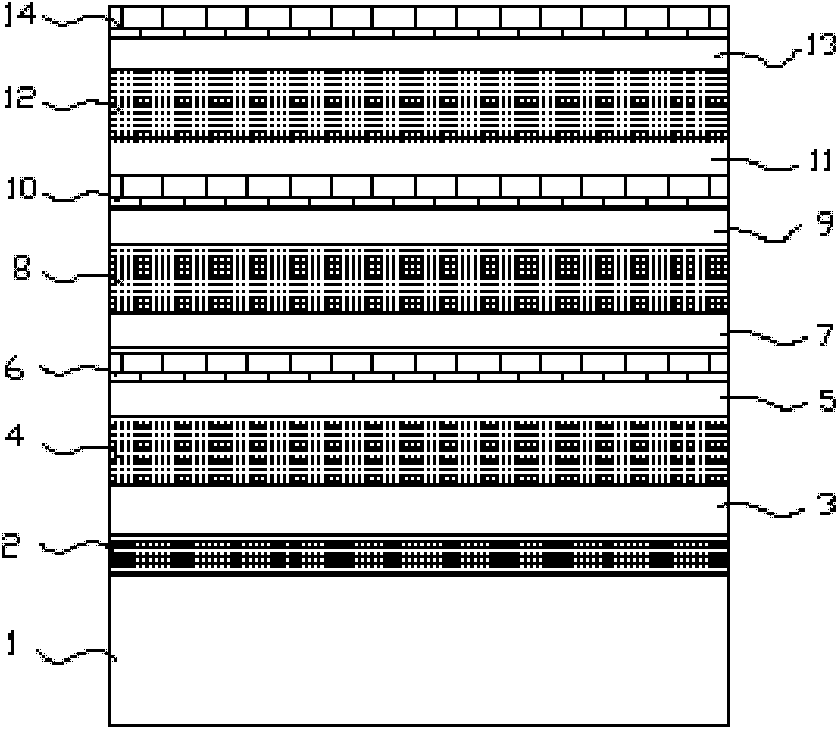
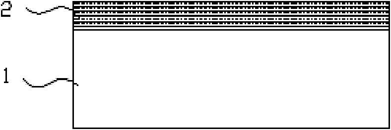
[0022] 1) Growth of Ge by high vacuum chemical vapor deposition x Si 1-x Stress transition layer: choose SiH 4 and GeH 4 as the source of the reaction. The (001) plane Si substrate 1 was cleaned, put into a high-vacuum chemical vapor deposition reaction chamber, and firstly baked at 1000° C. for 10 minutes. Then, the temperature was lowered to 600°C to grow Ge with Ge composition gradually changing from 0 to 1. x Si 1-x Stress transition layer 2 (such as figure 2 shown). During the growth process, the SiH 4 The flow rate is fixed, and then slowly increase the GeH 4 traffic. The growth temperature is 600° C., the growth pressure is 50 mTorr, the change rate of Ge content is 5% / μm, and the change mode is continuous change.

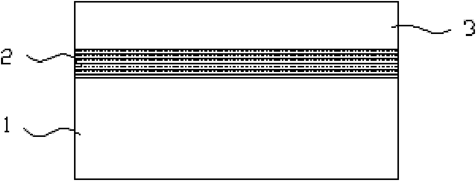
[0023] 2) in Ge x Si 1-x A Ge film layer 3 with a thickness of 2 μm is deposited on the stress transition layer (such as image 3 shown). The dislocation density of the Ge thin film layer 3 grown at this time is 5×10 6 cm -2 .

[0024] 3) F...

Embodiment 2

[0029] 1) Growth of Ge by high vacuum chemical vapor deposition x Si 1-x Stress transition layer: choose Si 2 h 6 and GeH 4 as the source of the reaction. The (001) plane Si substrate 1 was cleaned, put into a high-vacuum chemical vapor deposition reaction chamber, and firstly baked at 1000° C. for 10 minutes. Then, the temperature was lowered to 750°C, and Ge with Ge composition gradually changed from 0 to 1 was grown. x Si 1-x Stress transition layer 2 (such as figure 2 shown). During the growth process, the Si 2 h 6 The flow rate is fixed, and then slowly increase the GeH 4traffic. The growth temperature is 750°C, the growth pressure is 100mTorr, the change rate of Ge content is 8% / μm, and the change mode is a step change, and every growth of 0.5 μm is a step.

[0030] 2) in Ge x Si 1-x A Ge film layer 3 with a thickness of 2 μm is deposited on the stress transition layer (such as image 3 shown). The dislocation density of the Ge thin film layer 3 grown at...

Embodiment 3

[0036] 1) Growth of Ge by high vacuum chemical vapor deposition x Si 1-x Stress transition layer: choose Si 2 h 6 and GeH 4 as the source of the reaction. The (001) plane Si substrate 1 was cleaned, put into a high-vacuum chemical vapor deposition reaction chamber, and firstly baked at 1000° C. for 10 minutes. Then, the temperature was lowered to 800°C to grow Ge with Ge composition gradually changing from 0 to 1. x Si 1-x Stress transition layer 2 (such as figure 2 shown). During the growth process, the Si 2 h 6 The flow rate is fixed, and then slowly increase the GeH 4 traffic. The growth temperature is 800°C, the growth pressure is 300mTorr, the change rate of Ge content is 10% / μm, and the change method is a step change, and every 0.5 μm of growth is a step.

[0037] 2) in Ge x Si 1-x A Ge film layer 3 with a thickness of 2 μm is deposited on the stress transition layer (such as image 3 shown). The Ge thin film layer 3 grown at this time has a dislocation ...


PUM


Abstract

The invention provides a method for growing an InGaP/GaAs/Ge three-junction solar cell on a silicon substrate. The method comprises the following steps of: epitaxially growing a GexSi1-x stress transition layer with gradient components on the silicon substrate; forming a Ge thin film layer with fully relaxed stress on the stress transition layer; and performing the epitaxial growth to form the InGaP/GaAs/Ge three-junction solar cell comprising a bottom Ge sub-cell, a middle GaAs sub-cell and a top InGaP sub-cell on a Ge/GexSi1-x/Si template. By substituting the Si substrate of low cost for the expensive Ge substrate necessary for a conventional growth method, the method is used for the growth of the high-efficiency solar cell; and meanwhile, the InGaP/GaAs/Ge three-junction solar cell of larger area and lower defect density can be grown on the Si substrate so as to greatly reduce the production cost of the InGaP/GaAs/Ge three-junction solar cell.

Description

technical field [0001] The invention belongs to the field of epitaxial growth of compound semiconductor solar cells, in particular to a method for epitaxially growing high-quality InGaP / GaAs / Ge triple-junction high-efficiency solar cells on a silicon substrate. Background technique [0002] Due to the gradual depletion of non-renewable energy such as coal and oil and the continuous deterioration of the environment, human beings urgently need to use green energy to solve the huge problems they face. Solar cells manufactured using photoelectric conversion technology can directly convert solar energy into electrical energy, which greatly reduces people's dependence on coal, oil and natural gas in production and life, and has become one of the most effective ways to utilize green energy. [0003] III-V compound semiconductor multi-junction solar cells are the solar cells with the highest conversion efficiency. They also have the advantages of high temperature resistance, strong ...

Claims


Application Information

Patent Timeline
Patent Type & Authority Applications(China)
IPC IPC(8): H01L31/18
CPCY02P70/50
Inventor 吴志浩宋明辉陈长清方妍妍戴江南余晨辉熊晖
Owner HUAZHONG UNIV OF SCI & TECH
Why Eureka
Try Eureka