Level shifters, integrated circuits, systems, and method for operating the level shifters

A technology of voltage level shift and voltage level, which is applied in the direction of logic circuit, logic circuit interface device, logic circuit connection/interface layout, etc., and can solve problems such as limitations

Active Publication Date: 2010-10-13
TAIWAN SEMICON MFG CO LTD
View PDF2 Cites 17 Cited by
  • Summary
  • Abstract
  • Description
  • Claims
  • Application Information

AI Technical Summary

Problems solved by technology

Charge can be injected into or out of the floating gate, which becomes confined by the surrounding insulating material

Method used


Image

  • Level shifters, integrated circuits, systems, and method for operating the level shifters
  • Level shifters, integrated circuits, systems, and method for operating the level shifters
  • Level shifters, integrated circuits, systems, and method for operating the level shifters

Examples


Embodiment Construction

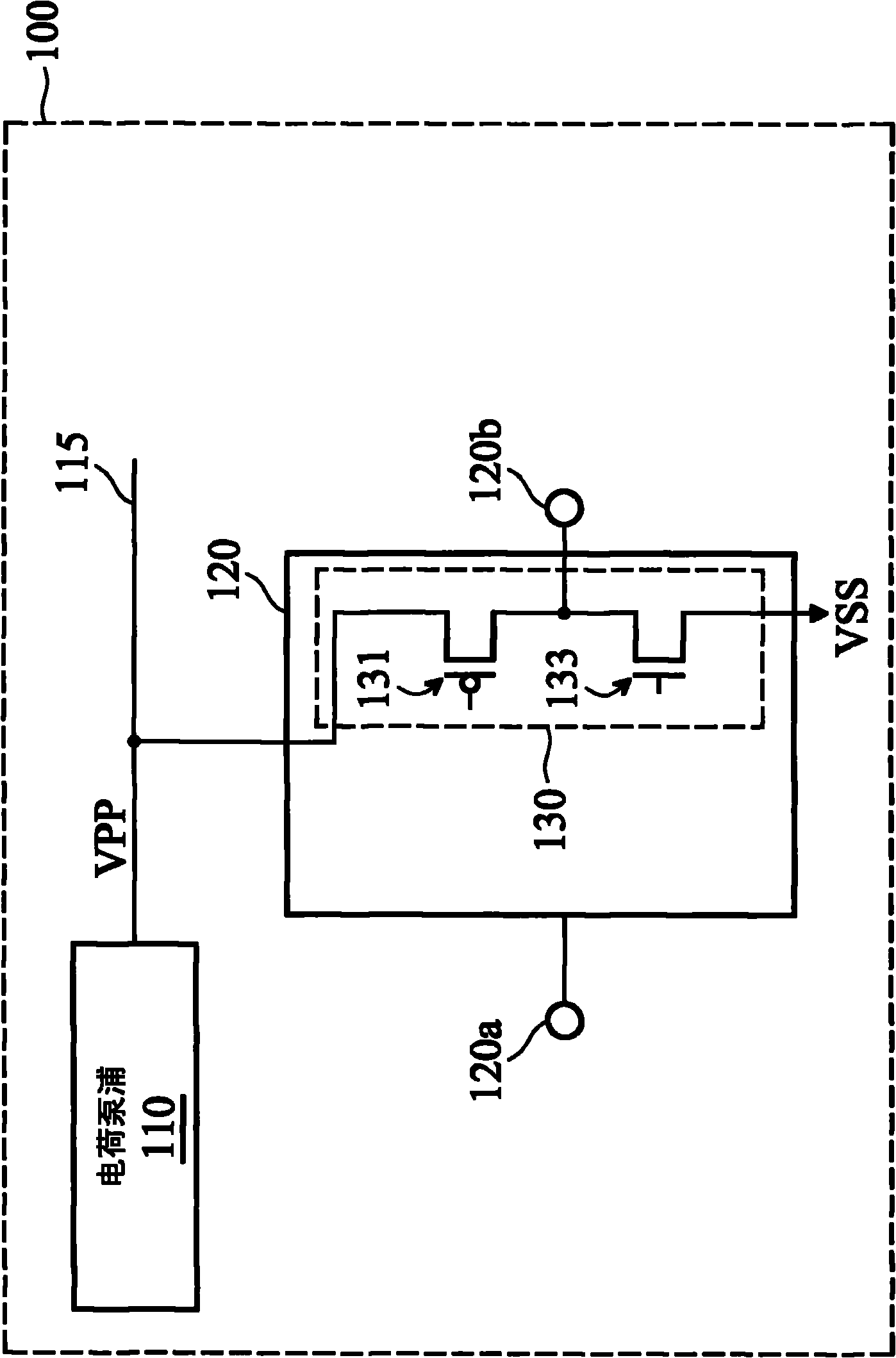
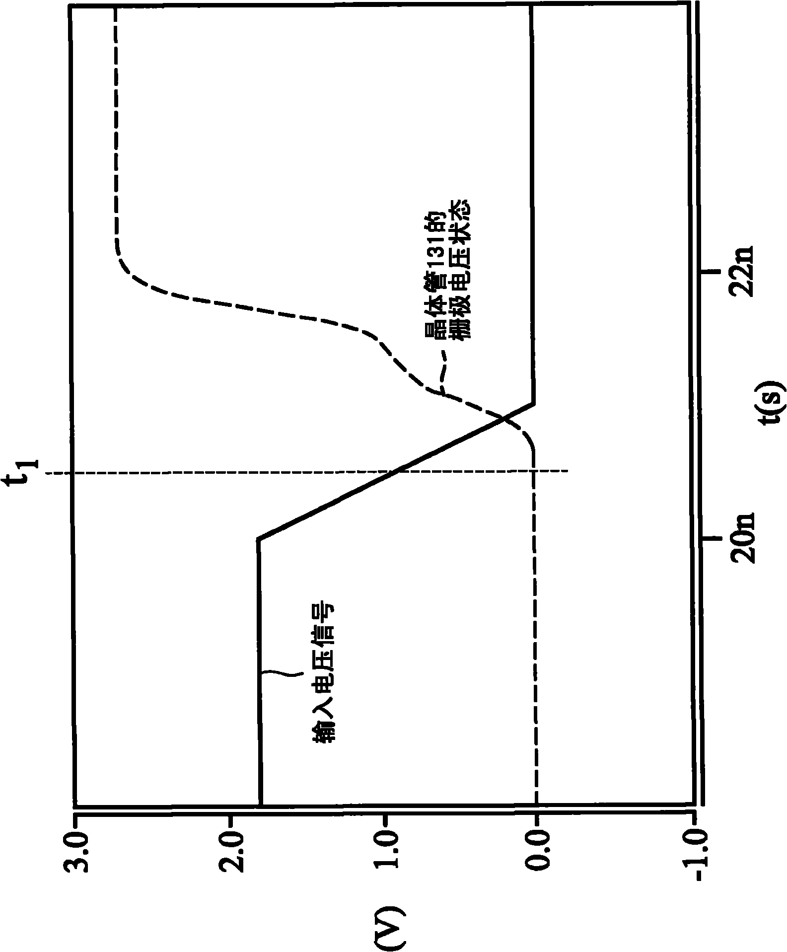
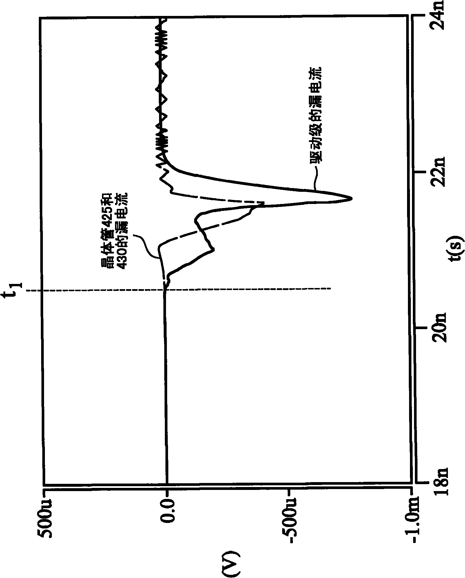
[0030] A common flash memory circuit has a voltage level shifter. The common voltage level shifter is like a high voltage switch, and the voltage level shifter is composed of a driver stage, an N-channel metal oxide semiconductor (NMOS) transistor N1, a P-channel A metal oxide semiconductor (PMOS for short) transistor P1 and an inverter are formed. The N-channel MOS transistor N1 and the P-channel MOS transistor P1 are coupled in series and configured in parallel with the driver stage. The inverter is coupled between the N-channel MOS transistor N1 and the driving stage, and the source terminal of the P-channel MOS transistor P1 is coupled to a low voltage VSS. When the input voltage signal is high, the output terminal of the driving stage outputs a high voltage HV; when the input voltage signal is low, the output terminal of the driving stage outputs a low voltage VSS.

[0031] A general driver stage is composed of an N-channel MOS transistor N2 and a P-channel MOS transist...


PUM


Abstract

The present invention provides level shifters, integrated circuits, systems, and a method for operating the level shifters. The level shifter includes an input end being capable of receiving an input voltage signal. The input voltage signal includes a first state transition from a first voltage state to a second voltage state. An output end can output an output voltage signal having a second state transition from a third voltage state to the second voltage state corresponding to the first state transition of the input voltage signal. A driver stage is coupled between the input end and the output end. The driver stage includes a first transistor and a second transistor. Substantially immediately from a time corresponding to about a mean of voltage levels of the first voltage state and the second voltage state, the second voltage state is substantially free from being applied to a gate of the first transistor so as to substantially turn off the first transistor. The present invention can avoid the flash device, the transistor and / or circuit damage under a high voltage operation.

Description

technical field [0001] The present invention relates to the field of a semiconductor circuit, in particular to a voltage level shifter, an integrated circuit, a system and a method for controlling level shifting. Background technique [0002] Flash memory is used in various applications, and flash memory provides random access and other processes to store data such as application programs. Data can be written and read multiple times from the flash memory unit, and the general flash memory unit is an improved metal-oxide-semiconductor transistor with stacked gates. The stacked gate includes a control gate and a floating gate, the control gate is used to control the conduction or non-conduction of the transistor to control the current from the drain (Drain) to the source (Source), and the floating gate is located at the control gate between the channel of the device. Charge can be injected into or out of the floating gate, which becomes confined by the surrounding insulating...

Claims


Application Information

Patent Timeline
Patent Type & Authority Applications(China)
IPC IPC(8): H03K19/0175
CPCH03K19/018521H03K19/017509H05K13/00Y10T29/49117
Inventor 杨天骏隋彧文林志昌普强荣
Owner TAIWAN SEMICON MFG CO LTD
Why Eureka
Try Eureka