Method of fabrication of a FINFET element

A component and device technology, applied in the field of semiconductor device manufacturing, can solve problems such as crystal quality problems and GOI substrates are not widely used

Inactive Publication Date: 2010-10-20
TAIWAN SEMICON MFG CO LTD
View PDF0 Cites 35 Cited by
  • Summary
  • Abstract
  • Description
  • Claims
  • Application Information

AI Technical Summary

Problems solved by technology

However, GOI substrates are not widely used in industrial processing
Additionally, GOI substrates can have crystal quality issues, especially at larger wafer sizes, e.g., 300mm wafers

Method used


Image

  • Method of fabrication of a FINFET element
  • Method of fabrication of a FINFET element
  • Method of fabrication of a FINFET element

Examples


Embodiment Construction

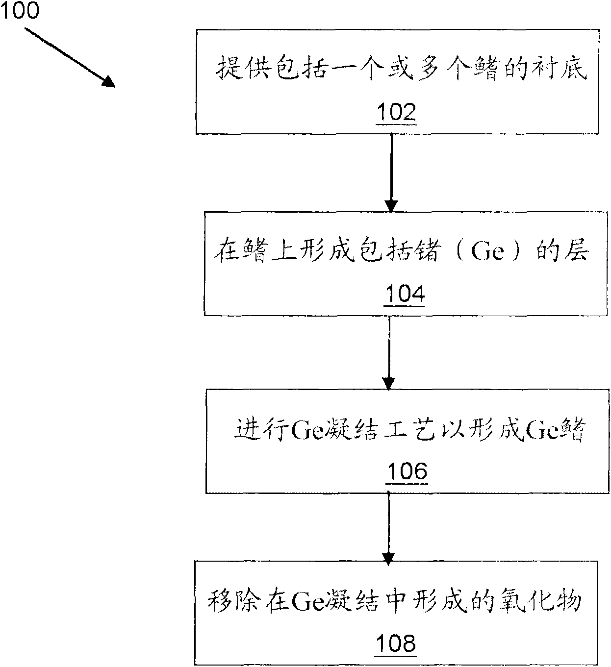
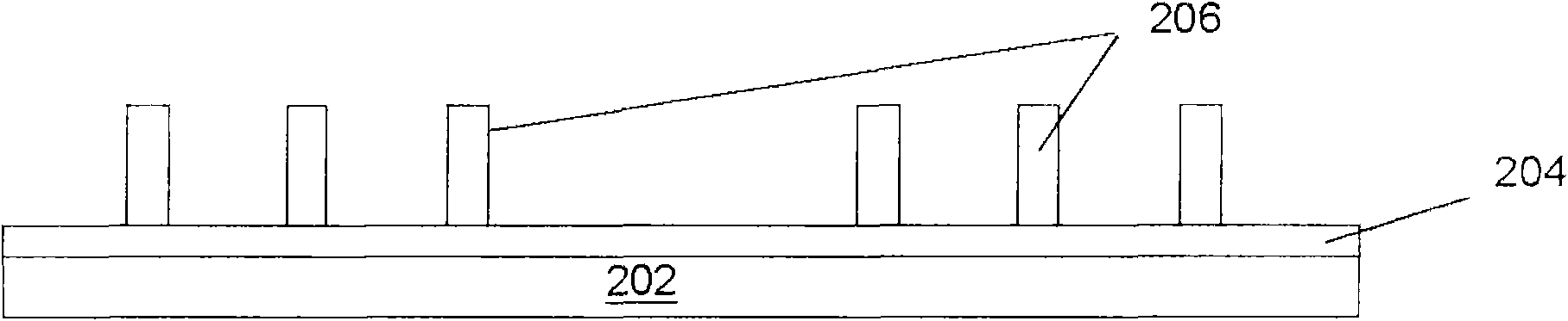
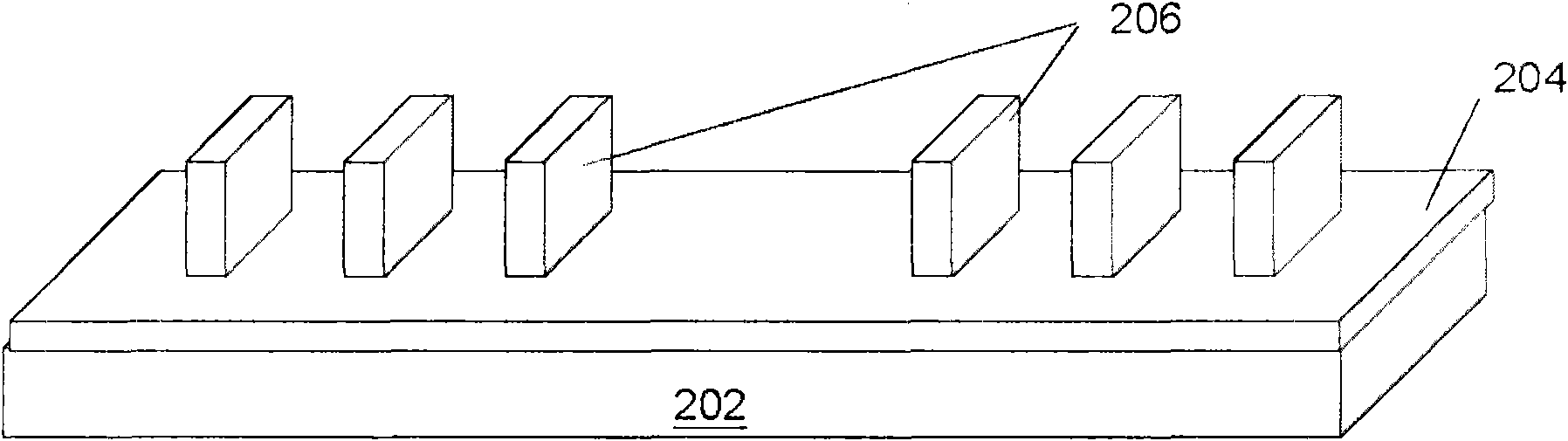
[0014] The present invention relates generally to semiconductor devices, and more particularly to FinFET components and methods of fabricating FinFET components (eg, devices or portions of devices). However, it is to be understood that the present invention provides specific embodiments as examples to teach broader inventive concepts, and those skilled in the art can readily apply the teachings of the present invention to other methods or devices. Additionally, it is to be understood that the methods and apparatuses discussed herein include some conventional structures and / or processes. Because these structures and processes are well known in the art, they are discussed only at a general level of detail. In addition, reference symbols are repeated in the drawings for the purpose of convenience and illustration, and such repetition does not indicate any necessary combination of features or steps in the drawings. In addition, the structure in which the first feature is on or ab...


PUM


Abstract

The present disclosure provides a FinFET element and a method of fabricating a FinFET element. The FinFET element includes a germanium-FinFET element (e.g., a multi-gate device including a Ge-fin). In one embodiment, the method of fabrication the Ge-FinFET element includes forming silicon fins on a substrate and selectively growing an epitaxial layer including germanium on the silicon fins. A Ge-condensation process may then be used to selectively oxidize the silicon of the Si-fin and transform the Si-fin to a Ge-fin. The method of fabrication provided may allow use of SOI substrate or bulk silicon substrates, and CMOS-compatible processes to form the Ge-FinFET element.

Description

technical field [0001] The present invention generally relates to the field of semiconductor device fabrication, and more particularly to methods of fabricating Fin Field Effect Transistors (FinFETs) or portions thereof. Background technique [0002] A dual-gate MOSFET is a MOSFET that includes two gates in one device. These devices are called FinFETs because their structure includes thin fins extending from the substrate. Silicon-based FinFETs can be successfully fabricated using conventional MOSFET technology. Typical FinFETs are fabricated on a substrate with an insulating layer above the substrate with thin fins extending from the substrate, eg, etched into the silicon layer of the substrate. The channel of the FET is formed in this vertical fin. Over (or around) the fins there is a gate. The benefit of a double gate is that having gates on both sides of the channel results in a gate that can control the channel from both sides. Additional benefits of FinFETs includ...

Claims


Application Information

Patent Timeline
Patent Type & Authority Applications(China)
IPC IPC(8): H01L21/84H01L21/8234H01L21/336H01L21/20H01L27/12H01L27/088H01L29/78
CPCH01L29/66795
Inventor 许俊豪
Owner TAIWAN SEMICON MFG CO LTD
Why Eureka
Try Eureka