Manufacture method of semiconductor nano-pillar array structure

A technology of nano-pillar array and fabrication method, which is applied in the field of preparation of semiconductor nanostructures and can solve problems such as difficulties in semiconductor nanostructures

Inactive Publication Date: 2010-10-27
INST OF SEMICONDUCTORS - CHINESE ACAD OF SCI
View PDF2 Cites 10 Cited by
  • Summary
  • Abstract
  • Description
  • Claims
  • Application Information

AI Technical Summary

Problems solved by technology

At present, it is common to pre-deposit a layer of metal on the bottom of the PAA template as a conductive layer, and prepare metal nanodots or nanowire arrays by electroplating. However, it is still difficult to prepare semiconductor nanostructures using PAA.

Method used


Image

  • Manufacture method of semiconductor nano-pillar array structure
  • Manufacture method of semiconductor nano-pillar array structure

Examples


Embodiment Construction

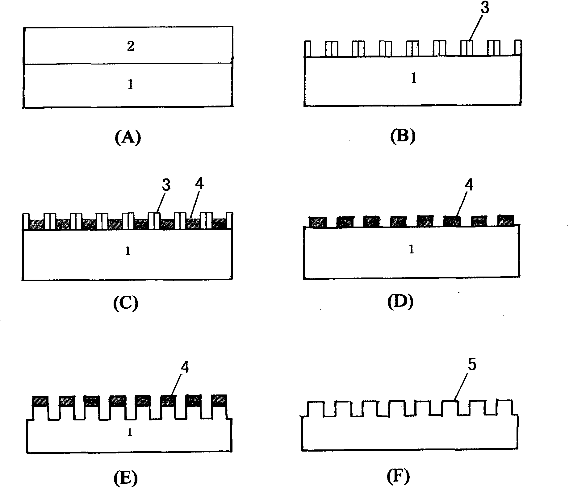
[0017] see figure 1 As shown, the present invention provides a method for manufacturing a semiconductor nanocolumn array structure, comprising the steps of:

[0018] Step 1: growing an aluminum layer 2 on a semiconductor substrate 1, such as figure 1 (A), the thickness of the aluminum layer 2 is 2 μm, the growth of the aluminum layer 2 is the method of electron beam evaporation, thermal evaporation or magnetron sputtering, and the semiconductor substrate is a group IV, III-V compound or II-VI Bulk materials or multi-layer structure materials of group compounds;

[0019] Step 2: anodize the aluminum layer 2 to form holes from the surface to the semiconductor substrate 1, forming a porous aluminum oxide film 3;

[0020] The anodic oxidation process adopts the secondary oxidation method. The specific method is to use the aluminum layer 2 as the anode and the platinum sheet as the cathode to perform the first oxidation in the electrolyte. The electrolyte is an aqueous oxalic aci...


PUM

PropertyMeasurementUnit
thicknessaaaaaaaaaa
thicknessaaaaaaaaaa

Abstract

The invention relates to a manufacture method of a semiconductor nano-pillar array structure, comprising the following steps of: 1. growing an aluminum layer on a semiconductor substrate; 2. carrying out anodic oxidation on the aluminum layer to form holes which are directly communicated with the semiconductor substrate from the surface so as to form a porous alumina film; 3. depositing metal on the surface of the porous alumina film and forming metal points in the holes of the porous alumina film; 4. carrying out wet etching on the porous alumina film so as to form a metal point array on the semiconductor substrate; and 5. carrying out etching on the semiconductor substrate by taking the metal point array as a mask film, removing the metal point array and forming a semiconductor nano-pillar array on the semiconductor substrate.

Description

technical field [0001] The invention relates to the preparation technology of semiconductor nanostructures, more specifically, the invention relates to a method of using porous anodic aluminum oxide film as a template, depositing metal dots in holes to realize pattern reverse transfer, and obtaining a semiconductor nanocolumn array structure. Background technique [0002] With the increasingly prominent application value of nanoscale devices in microelectronics, optics, and biochemistry, highly ordered low-dimensional array structures such as nanodots and nanopillars (nanowires) are due to the optical power brought by their quantum dimensions. , electric, magnetic and other properties are getting more and more attention. Commonly used methods for preparing nano-array structures include focused ion beam and electron beam exposure methods, self-organized growth methods, template methods and other methods. Focused ion beam and electron beam exposure methods have high cost, lon...

Claims


Application Information

Patent Timeline
Patent Type & Authority Applications(China)
IPC IPC(8): B82B3/00
Inventor 白安琪成步文左玉华王启明
Owner INST OF SEMICONDUCTORS - CHINESE ACAD OF SCI
Why Eureka
Try Eureka