Groove filling method

A filling method and groove technology, applied in gaseous chemical plating, coating, electrical components, etc., can solve problems such as film cracking

Active Publication Date: 2010-10-27
SHANGHAI HUAHONG GRACE SEMICON MFG CORP
View PDF5 Cites 18 Cited by
  • Summary
  • Abstract
  • Description
  • Claims
  • Application Information

AI Technical Summary

Problems solved by technology

In this way, the shrinkage of the film is more significant and the thermal stress is greater during the subsequent high-temperat

Method used


Image

  • Groove filling method
  • Groove filling method
  • Groove filling method

Examples


Embodiment Construction

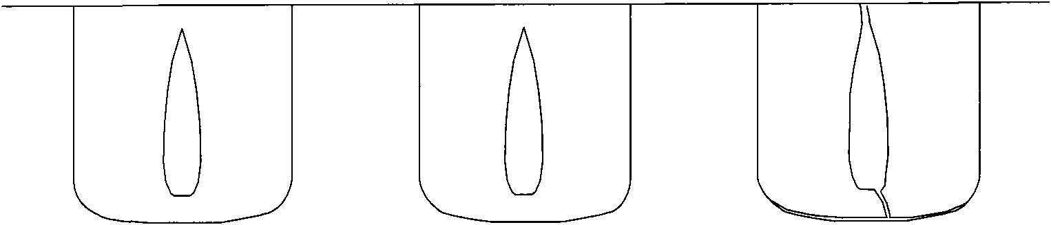
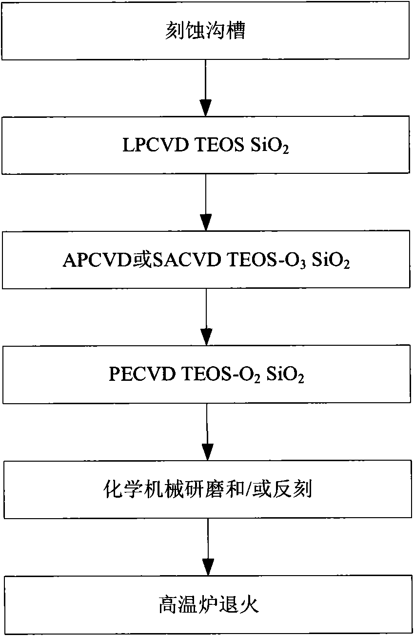
[0016] see figure 2 , the filling method of the groove of the present invention specifically comprises:

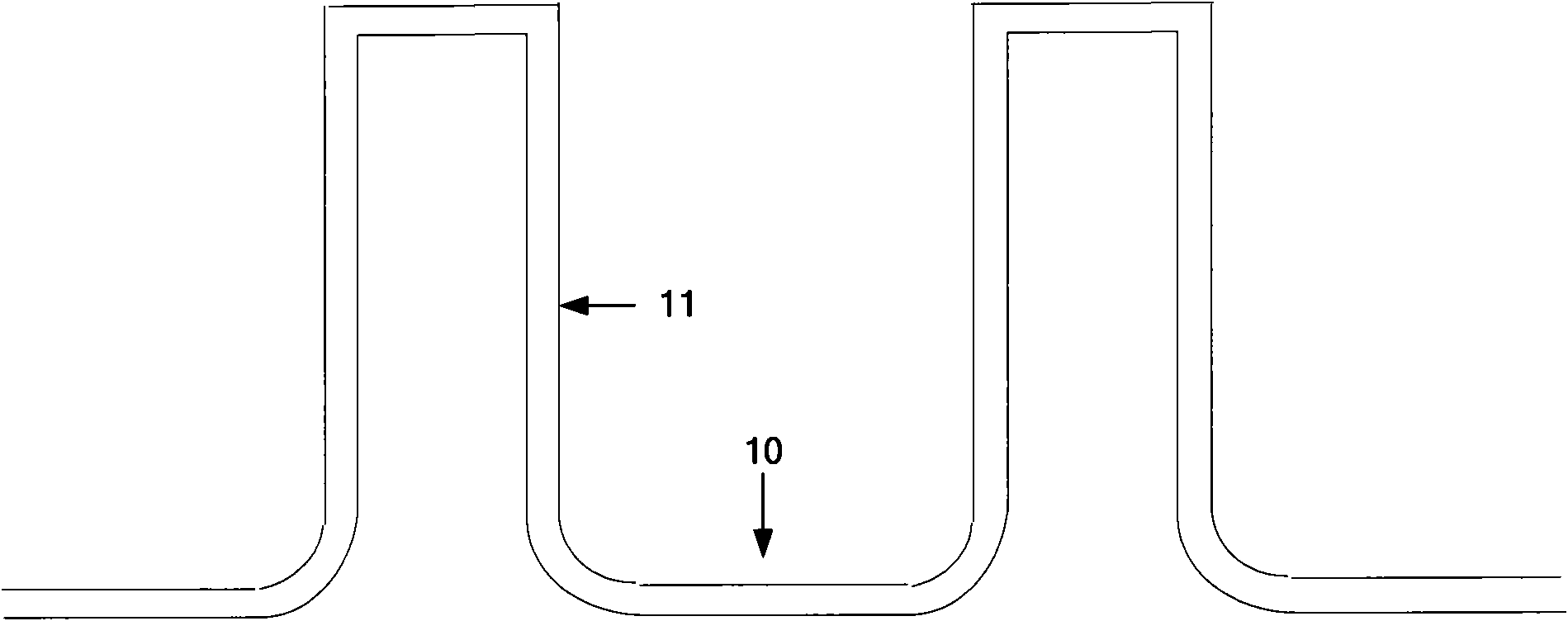
[0017] At the beginning, the surface of the silicon wafer has just etched the groove 10, and a layer of silicon dioxide (not shown) is thermally oxidized on the surface of the silicon wafer with the groove 10. The thickness of this layer of silicon dioxide is between 50 and between. This step is called thermal oxygen repair. In the semiconductor integrated circuit manufacturing process, thermal oxygen repair is an essential step after trench etching, and is used to restore the surface state of silicon after trench etching. Then a layer of silicon dioxide is deposited on the surface of the silicon wafer. This layer of silicon dioxide is a pad layer (not shown) with a thickness of 100- (The preferred value is 100~ ), used to improve the adhesion between silicon and trench fill (such as silicon dioxide).

[0018] Step 1, please refer to Figure 3a , on the surface of...


PUM


Abstract

The invention discloses a groove filling method. The width of a groove is above 1 mu m and the depth of the groove is above 3 mu m. The method comprises the following steps: step 1, using TEOS as a raw material to deposit a layer of SiO2 on the surface of a silicon slice with a groove by an LPCVD process; step 2, using TEOS and O3 as raw materials to deposit a layer of SiO2 again on the surface of the silicon slice by an APCVD or SACVD process; and step 3, using TEOS and O2 as raw materials to deposit a layer of SiO2 again on the surface of the silicon slice by the PECVD process. After the groove is filled according to the method of the invention, fillers in the groove are of a multilayer film structure; and the multilayer film structure is not cracked in a subsequent high-temperature furnace annealing process.

Description

technical field [0001] The invention relates to a semiconductor integrated circuit manufacturing process, in particular to a trench filling process. Background technique [0002] Using APCVD (atmospheric pressure chemical vapor deposition) process or SACVD (subatmospheric pressure chemical vapor deposition) process, TEOS (orthoethyl silicate, molecular formula Si(C) 2 h 5 O) 4 ) and O 3 (ozone) reacted deposited SiO 2 (Silicon dioxide) thin films have very good conformality and are widely used for trench filling in semiconductor integrated circuits. However, APCVD TEOS-O 3 SiO 2 thin film (that is, by APCVD process, by TEOS and O 3 SiO deposited as raw material 2 thin film) and SACVD TEOS-O 3 SiO 2 Thin films (i.e. by SACVD process, by TEOS and O 3 SiO deposited as raw material 2 film) has a large shrinkage rate in the subsequent high-temperature furnace annealing process, which will cause the SiO 2 A large stress is generated between Si (silicon) and Si (silico...

Claims


Application Information

Patent Timeline
IPC IPC(8): H01L21/762H01L21/764H01L21/316C23C16/44C23C16/40
Inventor 彭虎谢烜季伟缪燕
Owner SHANGHAI HUAHONG GRACE SEMICON MFG CORP
Why Eureka
Try Eureka