Photonic crystal rectangular coupled cavity zero dispersion slow optical wave guide

A photonic crystal, zero dispersion technology, applied in the direction of light guides, optics, optical components, etc., to achieve the effect of reducing the group velocity

Inactive Publication Date: 2010-11-17
INST OF SEMICONDUCTORS - CHINESE ACAD OF SCI
View PDF1 Cites 13 Cited by
  • Summary
  • Abstract
  • Description
  • Claims
  • Application Information

AI Technical Summary

Problems solved by technology

[0004] In view of this, the main purpose of the present invention is to provide a photonic crystal coupled cavity zero dispersion slow optical waveguide, to overcome the problem that the zero dispersion point of the photonic crystal coupled cavity slow optical waveguide is located in the light region, and to realize the slow optical single Modulo output

Method used


Image

  • Photonic crystal rectangular coupled cavity zero dispersion slow optical wave guide
  • Photonic crystal rectangular coupled cavity zero dispersion slow optical wave guide
  • Photonic crystal rectangular coupled cavity zero dispersion slow optical wave guide

Examples


Embodiment Construction

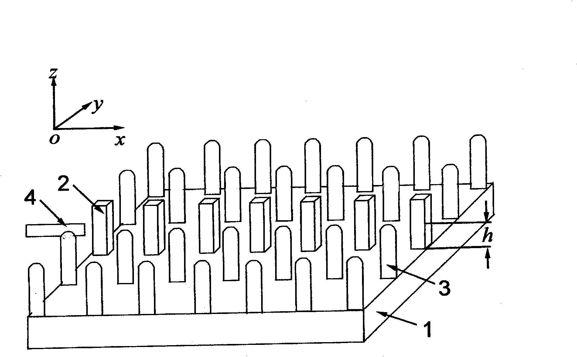
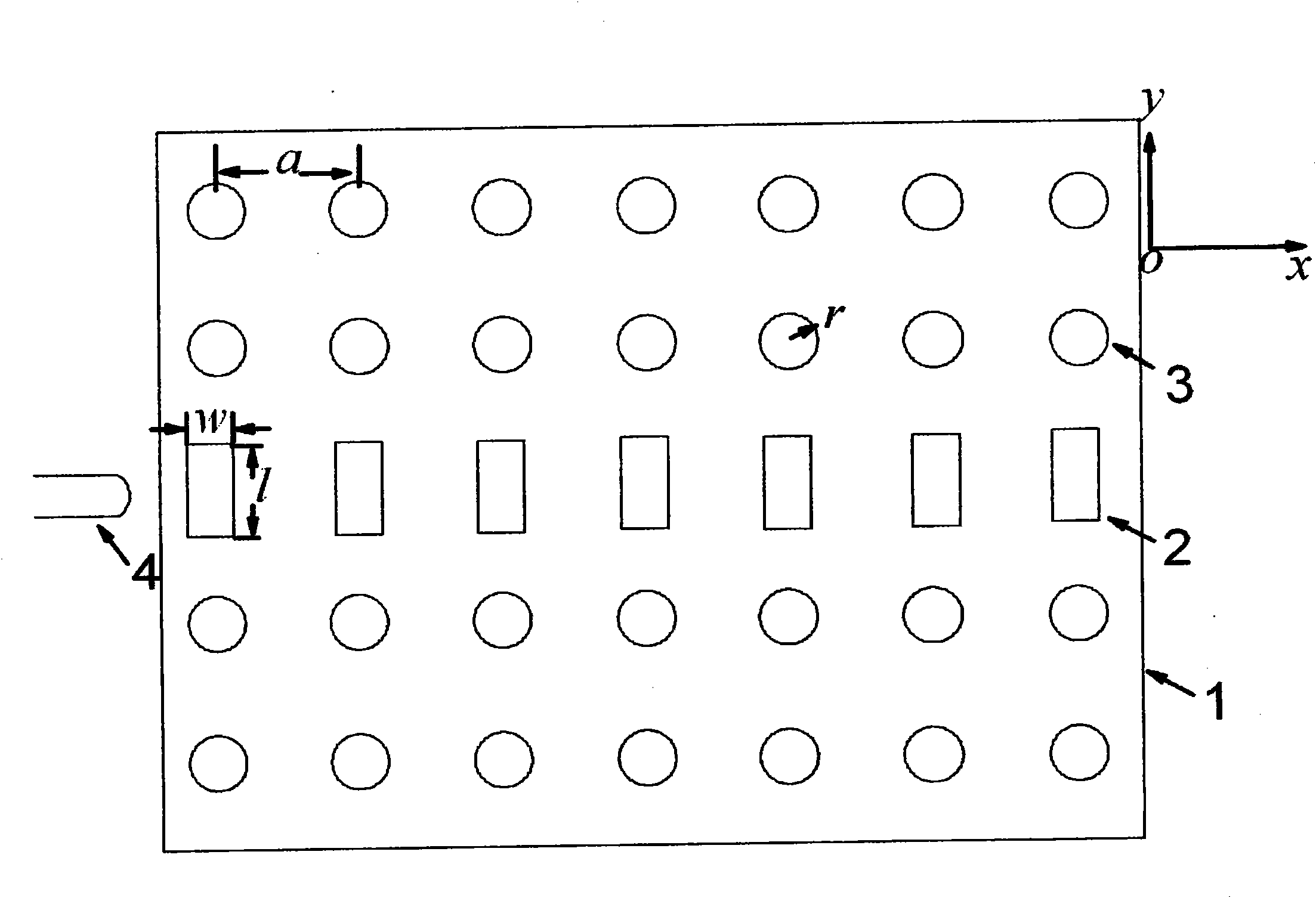
[0028] Such as figure 1 as shown, figure 1 The three-dimensional structure diagram of the photonic crystal zero-dispersion slow light waveguide provided for the present invention, the photonic crystal zero-dispersion slow light waveguide is composed of a substrate 1, a coupling cavity 2, and a dielectric column 3, and the excitation source 4 is located at h above the substrate.

[0029] in:

[0030] a substrate 1;

[0031] A plurality of coupling cavities 2, the coupling cavities 2 are rectangular cylinders, and the coupling cavities 2 are erected in a row on the middle part of the substrate 1, wherein the coupling cavities 2 are rectangular cavities; the rectangular coupling cavities 2 are single row along the The direction of photonic crystal single-line defect waveguide is arranged. For ordinary photonic crystal single-line defect waveguide, the mode in the forbidden band is monotonous. However, due to the existence of the rectangular coupling cavity, the mode in the phot...


PUM


Abstract

The invention provides a dielectric cylinder photonic crystal zero dispersion slow optical wave guide which comprises a substrate, a plurality of coupled cavities, a plurality of dielectric cylinders and an excitation source, wherein each coupled cavity is a rectangular cylinder, and the coupled cavities are vertically manufactured above the middle part of the substrate in a row and are used for regulating a slow light mode; each dielectric cylinder is a cylinder, and the dielectric cylinders are vertically manufactured above the substrate in a plurality of rows, are arranged at both sides of the coupled cavities and are used for laterally limiting a light field; and the excitation source is arranged at one side of the substrate, is relative to the coupled cavities in a row and excites the slow light mode to generate.

Description

technical field [0001] The invention relates to the technical field of semiconductor optoelectronic devices, in particular to a photonic crystal zero-dispersion slow light waveguide. Background technique [0002] Photonic crystal slow optical waveguide has been widely used in the fields of optical communication, optical storage, optical interconnection and biosensing due to its advantages of large potential bandwidth, realization at room temperature and two-dimensional array integration, which has aroused people's strong interest and interest. Closely. In many applications, the group velocity of the photonic crystal slow optical waveguide is required to be small enough, and the photonic crystal waveguide with single-line defects can achieve a larger bandwidth, but the corresponding group velocity is difficult to reduce, as document 1: "Mao XY, Zhang G Y , Huang YD et al..Chin.Phys.Lett., 2008, 25(12): 4311", the group velocity of single-defect waveguide in flat photonic cry...

Claims


Application Information

Patent Timeline
Patent Type & Authority Applications(China)
IPC IPC(8): G02B6/122
Inventor 曲连杰杨跃德黄永箴
Owner INST OF SEMICONDUCTORS - CHINESE ACAD OF SCI
Why Eureka
Try Eureka