Thermal interface material, electronic device with same and preparation method

一种热界面材料、电子装置的技术,应用在热交换的材料、化学仪器和方法、电路等方向,能够解决热阻大、热界面材料传热路径长、无法有效利用碳纳米管导热性能等问题,达到好导热性能、热阻小的效果

Active Publication Date: 2010-12-08
TSINGHUA UNIV +1
View PDF1 Cites 8 Cited by
  • Summary
  • Abstract
  • Description
  • Claims
  • Application Information

AI Technical Summary

Problems solved by technology

However, the direction of the plurality of carbon nanotubes in the flexible matrix is ​​difficult to control, and the probability that the axial direction of the carbon nanotubes is consistent with the heat transfer direction is very small. Therefore, more carbon nanotubes are required to overlap to form a heat conduction channel. , resulting in a long heat transfer path for the thermal interface material; and, due to the small size of the carbon nanotubes, the thermal resistance between the two overlapping carbon nanotubes is large, and the heat conduction of the carbon nanotubes cannot be effectively utilized. performance

Method used


Image

  • Thermal interface material, electronic device with same and preparation method
  • Thermal interface material, electronic device with same and preparation method
  • Thermal interface material, electronic device with same and preparation method

Examples


Embodiment Construction

[0015] The thermal interface material, the electronic device with the thermal interface material and the manufacturing method of the electronic device according to the embodiments of the present invention will be further described in detail below with reference to the accompanying drawings.

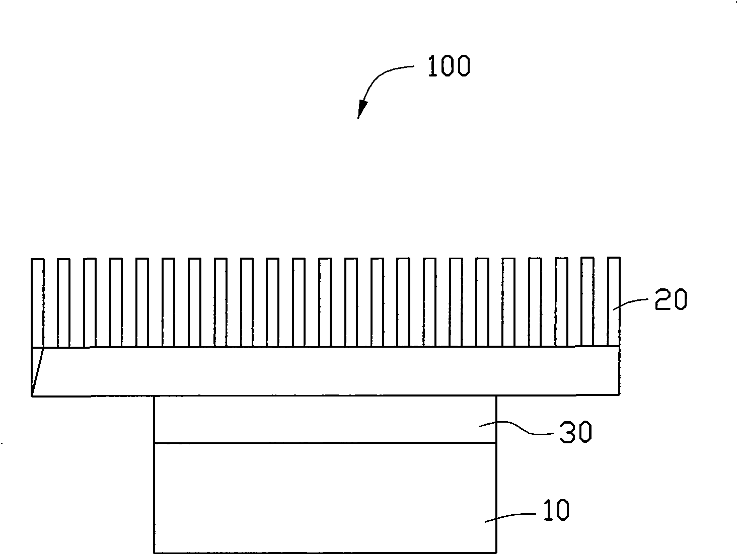
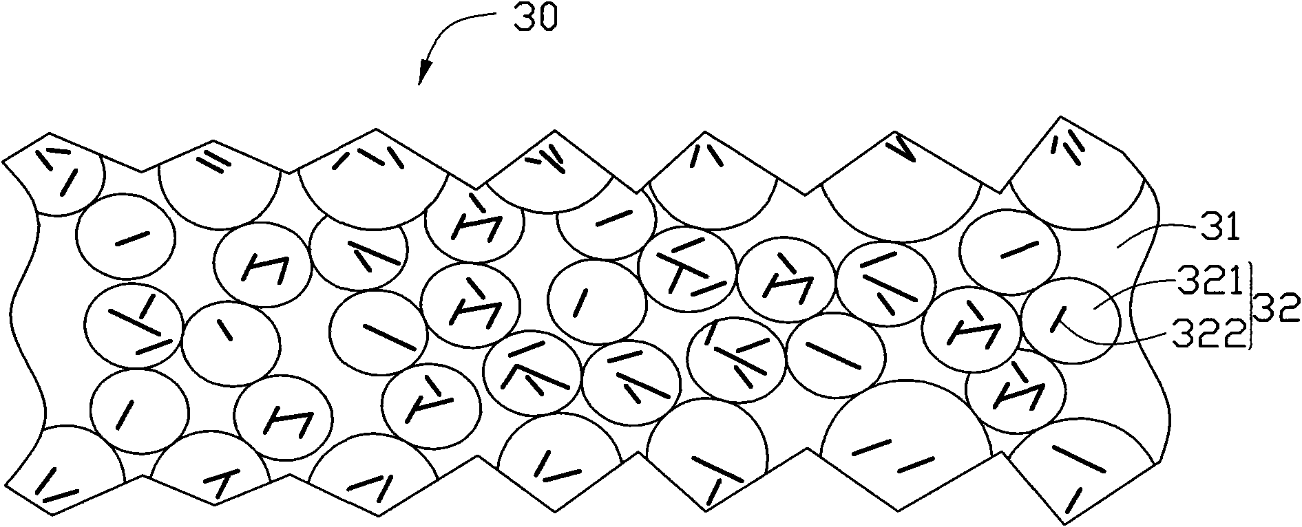
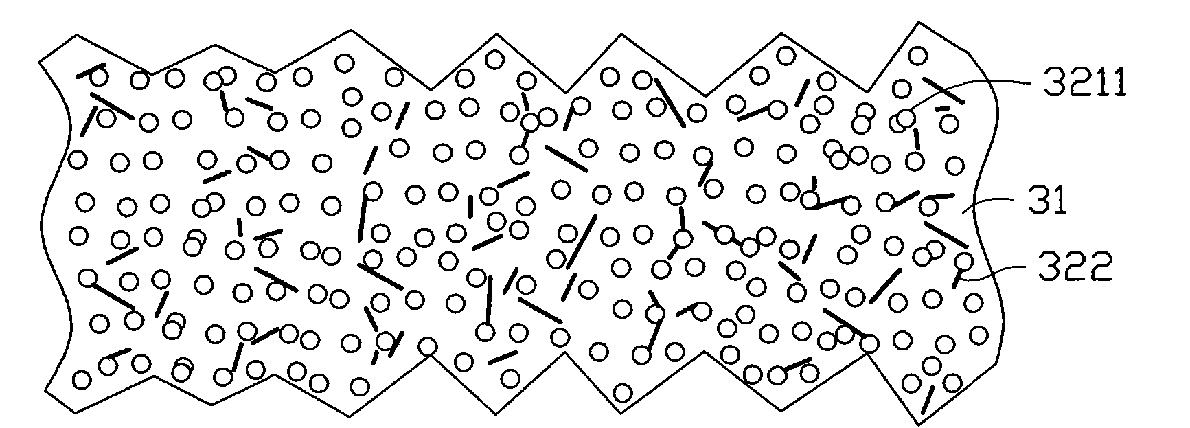
[0016] see figure 1 , is the electronic device 100 provided by the embodiment of the present invention, which includes a heat source 10, a heat dissipation device 20 and a thermal interface material 30, and the thermal interface material 30 is arranged between the heat source 10 and the heat dissipation device 20 for The heat generated by the heat source 10 is transferred to the heat sink 20 .

[0017] The heat source 10 may be a semiconductor integrated device, or an IC circuit, a resistor or other heating elements. The heat source 10 has a protection temperature T1 that prevents the heat source 10 from being damaged by overheating. It can be understood that when the temperature of the...


PUM

PropertyMeasurementUnit
particle diameteraaaaaaaaaa

Abstract

The invention relates to a thermal interface material which comprises a flexible matrix and a plurality of composite thermal conduction particles distributed in the flexible matrix, wherein each composite thermal conduction particle comprises a first metal particle and at least one carbon nano tube compounded in the first metal particle. In the thermal interface material, the plurality of composite thermal conduction particles are mutually lap jointed to form a thermal conduction channel, thus the material has shorter thermal transfer path; and moreover, because the composite thermal conduction particles have larger grain sizes, thermal resistance among the mutually lap jointed thermal conduction particles is small. The invention also relates to an electronic device with the thermal interface material and a preparation method of the electronic device.

Description

technical field [0001] The invention relates to a thermal interface material, an electronic device with the thermal interface material and a preparation method of the electronic device. Background technique [0002] In recent years, with the rapid development of the integration process of semiconductor devices, the degree of integration of semiconductor devices has become higher and higher, and the volume of devices has become smaller and smaller. However, the reduction in the volume of semiconductor devices has also increased its requirements for heat dissipation. In order to meet the heat dissipation requirements of the semiconductor devices, various heat dissipation methods such as fan heat dissipation, water-cooled auxiliary heat dissipation, and heat pipe heat dissipation are widely used, and certain heat dissipation effects have been obtained. However, because the contact interface between the heat sink and the heat source (semiconductor integrated device, such as CPU)...

Claims


Application Information

Patent Timeline
Patent Type & Authority Applications(China)
IPC IPC(8): C09K5/14H01L23/373H01L21/48
CPCC09K5/14H01L2924/0105H01L2924/01082H01L2224/29344H01L24/32H01L23/373H01L2224/29347H01L2924/01029H01L2924/00013H01L2224/29H01L2924/19041H01L2924/01013H01L2224/29393H01L2224/29298H01L2224/29339H01L2924/0665H01L2224/2919H01L2224/2929H01L2924/19043H01L2924/01047H01L2924/01079H01L2224/29311H01L2224/838H01L2924/14H01L24/83H01L24/29H01L2924/01005H01L2924/01033H01L2924/01006H01L23/42H01L2924/01078H01L23/3737H01L2224/293H01L2224/29499H01L2224/32245H01L2224/83365H01L2224/83385H01L2224/8385Y10T428/25Y10T428/12993H01L2924/00014H01L2924/00H01L2224/29099H01L2224/29199H01L2224/29299
Inventor 汪友森姚湲戴风伟王继存张慧玲
Owner TSINGHUA UNIV
Why Eureka
Try Eureka