Method for fabricating integrated circuit

A technology of integrated circuits and manufacturing methods, applied in the fields of circuits, semiconductor/solid-state device manufacturing, electrical components, etc., can solve the problems of reducing the quality of patterned outlines, damage to the conductive layer, etc., to improve the overall device performance, shape, and resistance. The effect of adhesion

Active Publication Date: 2010-12-08
TAIWAN SEMICON MFG CO LTD
View PDF0 Cites 16 Cited by
  • Summary
  • Abstract
  • Description
  • Claims
  • Application Information

AI Technical Summary

Problems solved by technology

However, it has been observed that: the dry etching process causes damage to the high dielectric constant layer and the conductive layer, and sometimes l

Method used


Image

  • Method for fabricating integrated circuit
  • Method for fabricating integrated circuit
  • Method for fabricating integrated circuit

Examples


Embodiment Construction

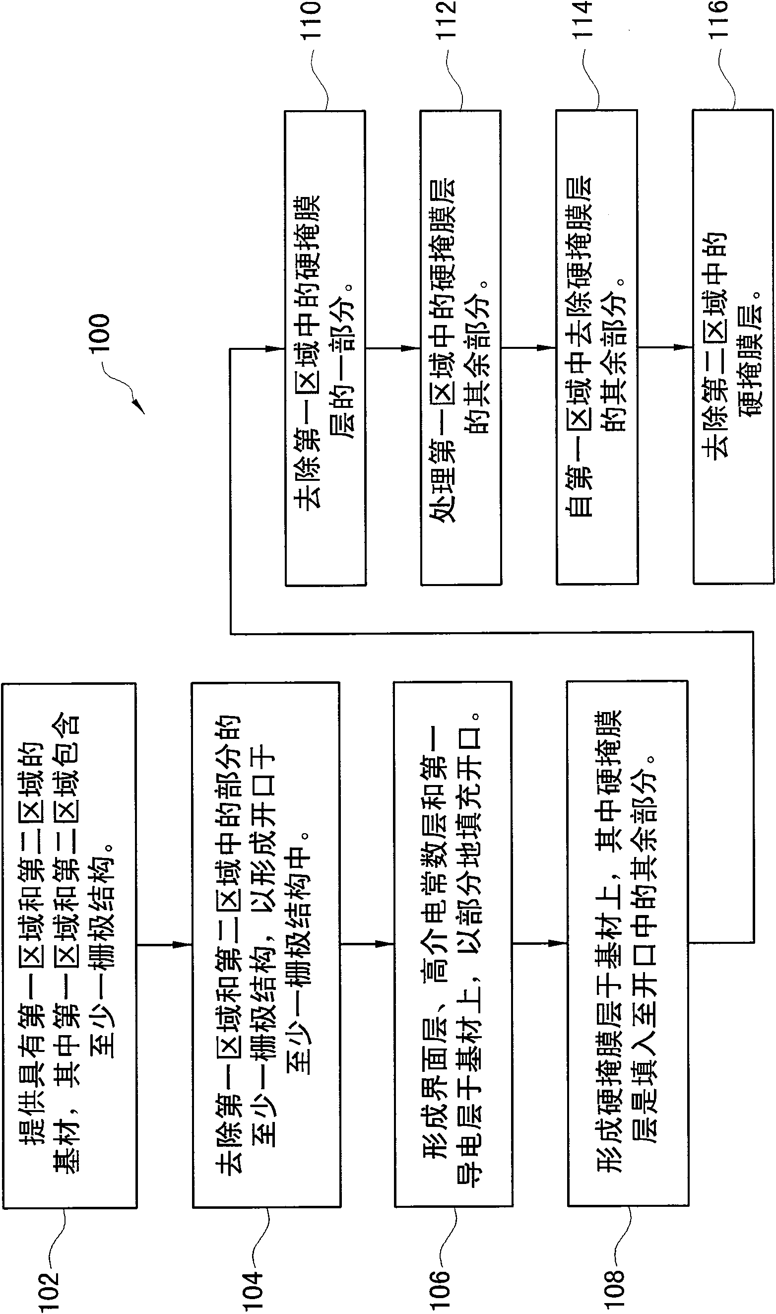
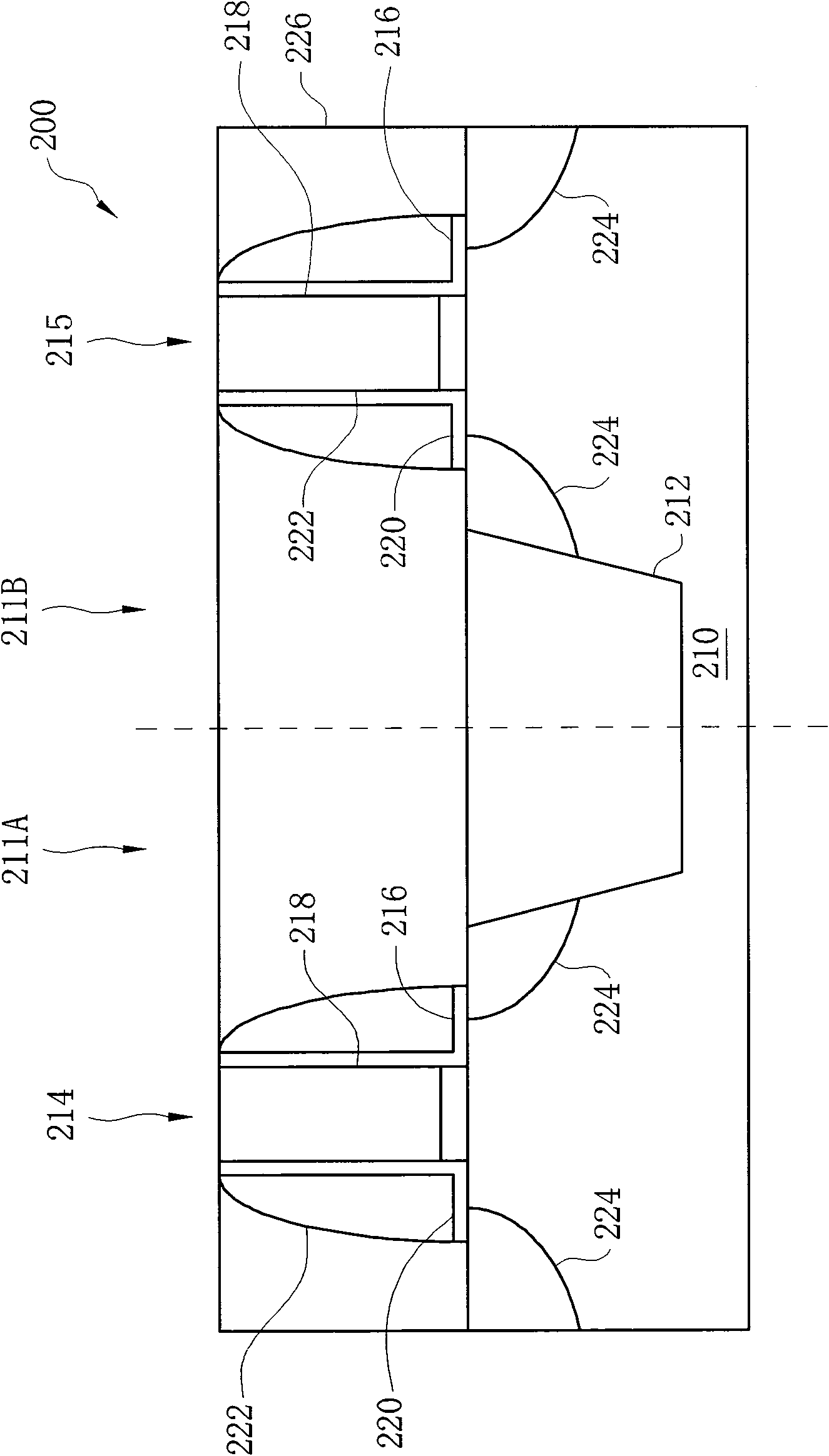
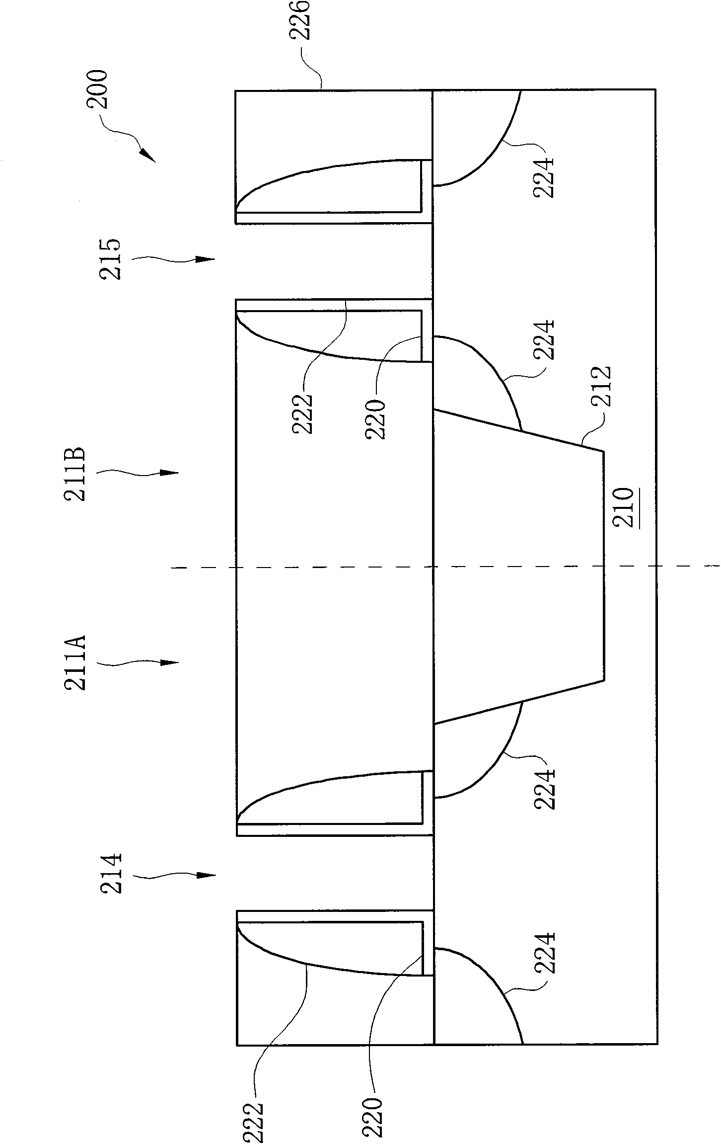
[0034] The present disclosure generally relates to a method of manufacturing an integrated circuit. In particular, it relates to a method of fabricating integrated circuits with improved etch selectivity.

[0035] It is to be understood that the following disclosure provides many embodiments or illustrations for implementing different features of the invention. Specific illustrations of components and arrangements are described below to simplify the present disclosure. These illustrations are of course only for illustration, and are not intended to limit the present invention. For example: the first feature described below on or above the second feature may include an embodiment in which the first feature and the second feature are in direct contact; it may also include an embodiment in which an additional feature is formed between the first feature and the second feature Embodiments so that the first feature and the second feature are not in direct contact. In addition, th...


PUM

PropertyMeasurementUnit
Thicknessaaaaaaaaaa

Abstract

A method for fabricating an integrated circuit with improved performance is disclosed. The method comprises providing a substrate; forming a hard mask layer over the substrate; forming a photoresistance layer on the hard mask layer; patterning the photoresistance layer on the hard mask layer so as to limit a plurality of protected portions and a plurality of unprotected portions on the hard mask layer; performing a first etching process, a second etching process, and a third etching process on the unprotected portions of the hard mask layer, wherein the first etching process partially removes the unprotected portions of the hard mask layer, the second etching process corrects etching selectivity of the other unprotected portions compared with the protected portions of the hard mask layer, and the third etching process removes the remaining unprotected portions of the hard mask layer; and performing a fourth etching process to remove the protected portions of the hard mask layer.

Description

technical field [0001] The invention relates to a manufacturing method of an integrated circuit. In particular, the present invention relates to a method of manufacturing an integrated circuit capable of improving etching selectivity. Background technique [0002] The semiconductor integrated circuit manufacturing industry has experienced rapid growth. In the evolution of integrated circuits, when the geometric size (that is, the smallest component or line width that can be made using a process) has decreased, the functional density (Functional Density; that is, the number of interconnected components per chip area) has generally increased. number). This scaling down process generally provides benefits by increasing production efficiency and reducing associated costs. This shrinking process has also resulted in the adoption of high dielectric constant layers and conductive layers (eg, metal layers) to form various integrated circuit components (eg, Metal-Oxide-Semiconduct...

Claims


Application Information

Patent Timeline
IPC IPC(8): H01L21/70H01L21/28
CPCH01L29/4966Y10S438/942H01L29/513H01L29/66545H01L29/517H01L21/823842
Inventor 蔡方文叶明熙王明俊林舜武陈启群魏正泉陈其贤
Owner TAIWAN SEMICON MFG CO LTD
Why Eureka
Try Eureka