Supercharge Your Innovation With Domain-Expert AI Agents!

Method for manufacturing TFT substrate for current control

A manufacturing method and current control technology, applied in semiconductor/solid-state device manufacturing, circuits, electrical components, etc., can solve problems such as the inability to achieve high frequency

Inactive Publication Date: 2010-12-15
IDEMITSU KOSAN CO LTD
View PDF6 Cites 0 Cited by
  • Summary
  • Abstract
  • Description
  • Claims
  • Application Information

AI Technical Summary

Problems solved by technology

In this way, in order to increase the frequency of AC drive, it is necessary to increase the frequency of scanning, and there is a problem that high frequency cannot be achieved.

Method used


Image

  • Method for manufacturing TFT substrate for current control
  • Method for manufacturing TFT substrate for current control
  • Method for manufacturing TFT substrate for current control

Examples


no. 2 Embodiment approach

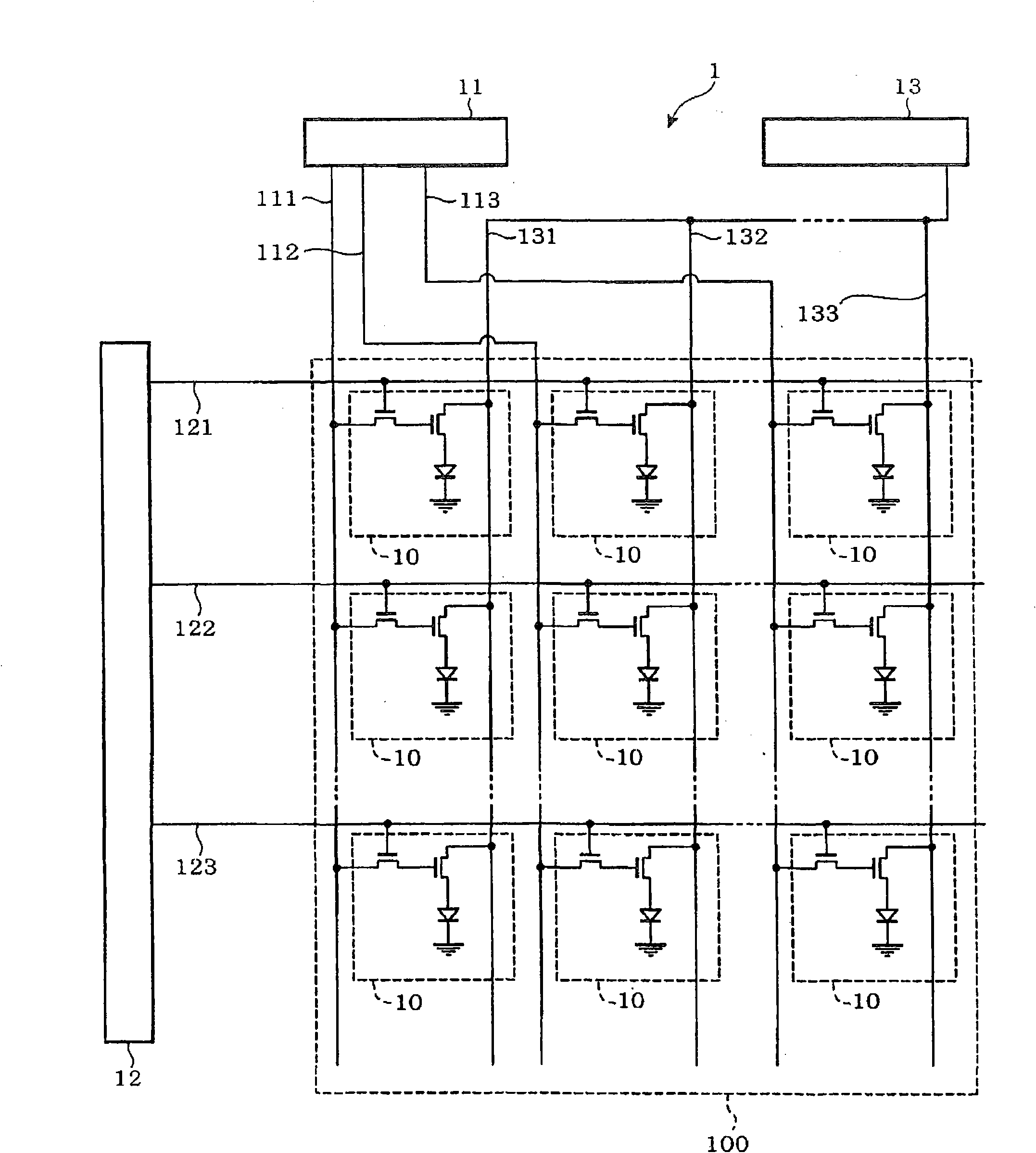
[0235] Figure 17 It is a block diagram showing the configuration of the organic EL display device according to the first embodiment of the present invention.

[0236] exist Figure 17Among them, the organic EL display device 1a as an electro-optical device includes a data line drive circuit 11, a scan line drive circuit 12, a power line control circuit 13a, a current measurement circuit 15, and a current control TFT substrate 100a (abbreviated as "TFT" as appropriate). substrate 100a"). In addition, m (column: m is a natural number)×n (row: n is a natural number) pixels 10 a are arranged in an array on the TFT substrate 100 .

[0237] The data line drive circuit 11 is connected to each pixel 10a through the first data line 111, the second data line 112...the mth data line 113 as a medium. The data line drive circuit 11 outputs a data signal to each pixel 10a.

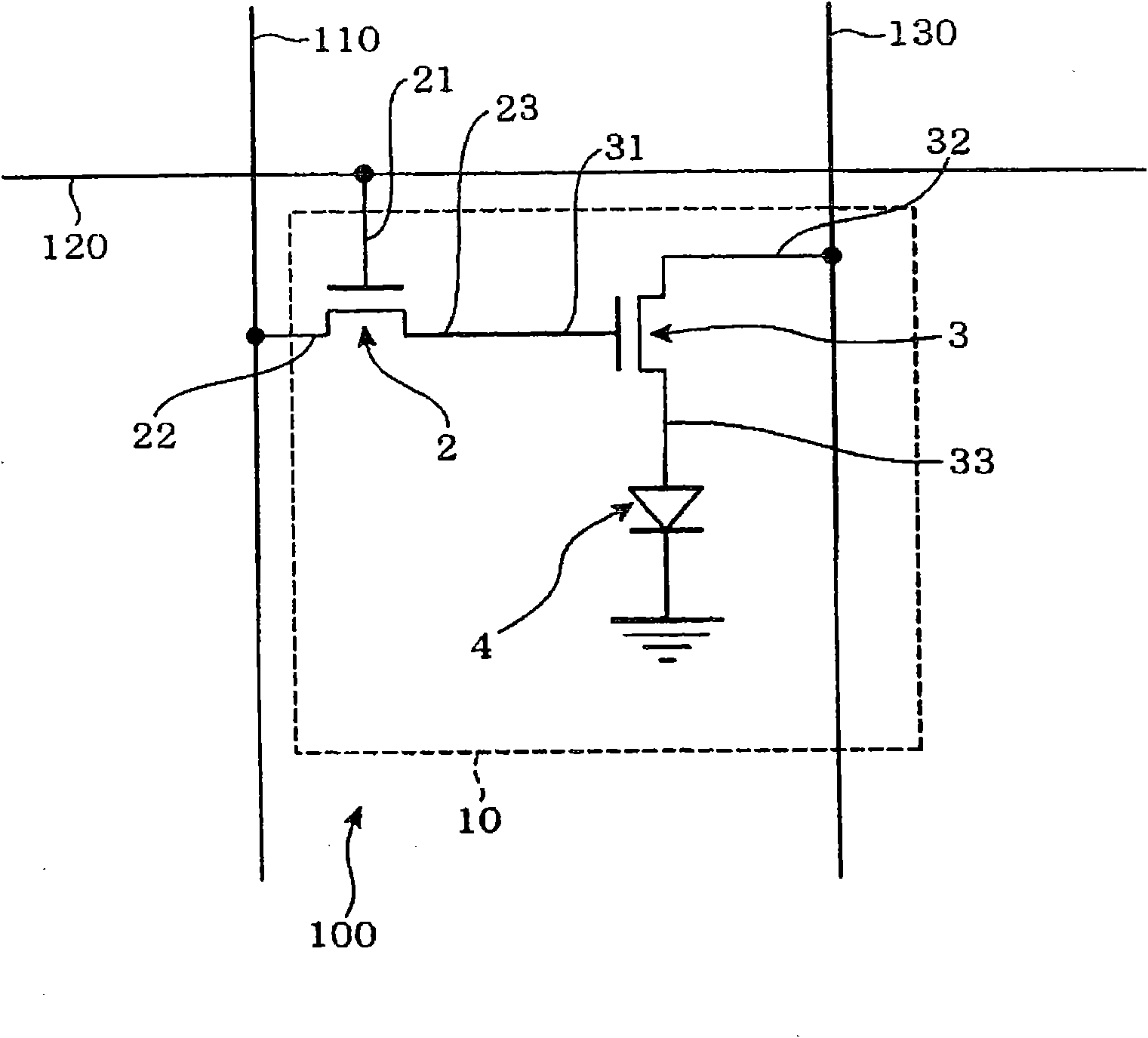
[0238] In addition, the scanning line driving circuit 12 is connected to each pixel 10 a through the first scann...


PUM


Abstract

A method for manufacturing TFT substrate for current control comprises: laminating a conductor layer and a first resist layer, forming scan lines, switching tube grids and grid lines by a first mask; laminating the switching tube grids insulation film; laminating an active layer having amorphous Si or polycrystalline Si or oxide semiconductor layer, a conductor layer and a second resist layer, forming data lines, switching tube source electrode lines, source electrodes, channel portions, drain electrodes, drain electrode lines, driving tube grid lines and gate electrodes; laminating the driving tube grids insulation film; laminating an oxide semiconductor layer and a third resist layer, forming a driving pipe active layer by a third mask; laminating an oxide conductor layer and a fourth resist layer, forming EL driving lines, driving tube source electrode lines, source electrodes, channel portions, drain electrodes, drain electrode lines and pixel electrodes; and a laminating insulation protective film and a fifth resist layer, and exposing scan line used bosses, data line used bosses, EL driving line used bosses and pixel electrodes by a fifth mask.

Description

[0001] This application is a divisional application with application number 200780013174.X (application date: 2007.4.10; invention name: electro-optical device, TFT substrate for current control and manufacturing method thereof). technical field [0002] The present invention relates to an electro-optical device, a TFT substrate for current control, and a manufacturing method thereof. In particular, by adopting the electro-optic device, the TFT substrate for current control and the manufacturing method thereof, the alternating current can be directly controlled, the high-frequency alternating current can be output, and the large power can be stably output, thereby reducing the manufacturing cost. Background technique [0003] An organic EL display device is attracting attention as a next-generation display device and solid-state lighting that will replace an LCD (Liquid Crystal Display) display device. The reason for this is that since the organic EL (Electronic Luminescence...

Claims


Application Information

Patent Timeline
Patent Type & Authority Applications(China)
IPC IPC(8): H01L21/77H01L27/32H01L27/02
CPCG09G3/3233G09G2320/043H01L27/1288H01L29/7869G09G2320/029G09G2300/0852G09G2300/0417H01L27/1255H01L29/45G09G2320/0295H01L27/1214H01L27/1225G09G2300/0842H01L27/124H10K59/131
Inventor 井上一吉矢野公规田中信夫
Owner IDEMITSU KOSAN CO LTD
Features
  • R&D
  • Intellectual Property
  • Life Sciences
  • Materials
  • Tech Scout
  • Unparalleled Data Quality
  • Higher Quality Content
  • 60% Fewer Hallucinations
Learn More