Wafer grinding method

A grinding method and wafer technology, applied in the direction of grinding devices, grinding machine tools, precision positioning equipment, etc., can solve the problems of weak strength, cracking, silicon slag easily stuck in the opening 102, etc., and achieve the effect of improving the yield rate

Active Publication Date: 2010-12-29
ADVANCED SEMICON ENG INC
View PDF0 Cites 5 Cited by
  • Summary
  • Abstract
  • Description
  • Claims
  • Application Information

AI Technical Summary

Problems solved by technology

However, during the grinding process, the cracked areas A, B of the wafer (such as the edge of the wafer) cause cracks due to weakened strength, and the silicon slag 104 is easily stuck in the opening 102

Method used


Image

  • Wafer grinding method
  • Wafer grinding method
  • Wafer grinding method

Examples


Embodiment Construction

[0023] In order to make the above-mentioned objects, features and advantages of the present invention more obvious and easy to understand, the preferred embodiments of the present invention are exemplified below, and are described in detail as follows in conjunction with the accompanying drawings:

[0024] Please refer to Figures 2A to 2F It is a schematic diagram of a wafer grinding method according to an embodiment of the present invention. Please refer to the following steps:

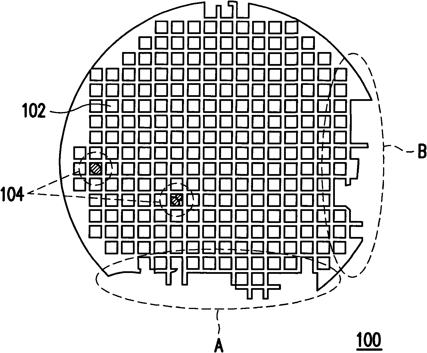
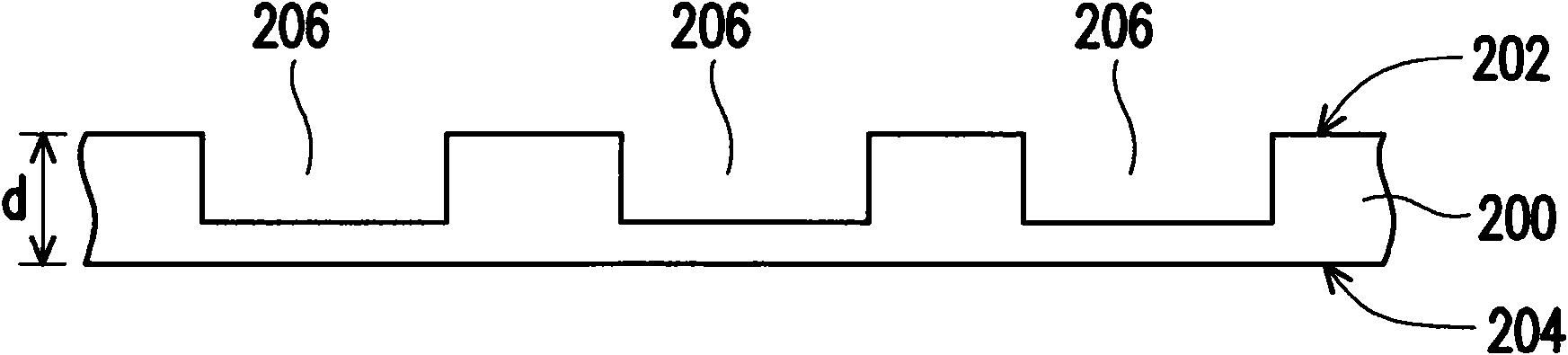
[0025] First, the first step is to provide a wafer 200, the wafer has a first surface 202, a second surface 204 and a plurality of openings 206 recessed in the first surface 202, and the wafer 200 has a thickness d.

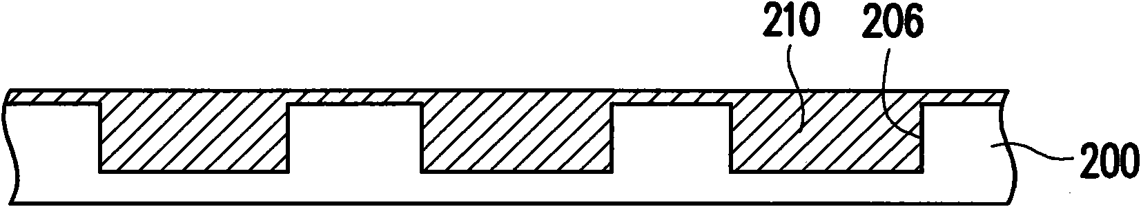
[0026] Please refer to Figure 2A , in the first step of this embodiment, dry etching or wet etching is performed on the first surface 202 of the wafer 200, so that a plurality of openings 206 (or cavities) are formed on the first surface 202 of the wafer 200, The depths of these op...


PUM


Abstract

The invention discloses a wafer grinding method which comprises the following steps of: firstly, providing a wafer which is provided with a first side, a second side and a plurality of opening parts sunk in the first side; filing plastic rubber in the opening parts and solidifying the plastic rubber; and grinding to reduce the thickness of the wafer. Since the wafer is protected by the plastic rubber during grinding, the yield of the wafer is improved.

Description

【Technical field】 [0001] The present invention relates to a wafer grinding method, and particularly relates to a wafer grinding method for preventing wafer breakage. 【Background technique】 [0002] Micro-Electro-Mechanical Systems (MEMS) are tiny electro-mechanical components fabricated in miniaturized packages. They are fabricated using techniques very similar to those used to fabricate integrated circuits, but MEMS devices interact with their environment in more ways than traditional Integrated circuits, such as mechanical, optical or magnetic interactions. [0003] MEMS devices can include extremely small electromechanical elements (such as switches, mirrors, capacitors, accelerometers, sensors, capacitive sensors, or actuators, etc.), while MEMS devices can be integrated with integrated circuits in a monolithic manner, while greatly improving the overall Insertion loss and galvanic isolation of solid-state devices. However, MEMS devices are extremely fragile in the mac...

Claims


Application Information

Patent Timeline
Patent Type & Authority Applications(China)
IPC IPC(8): B24B37/04B81C3/00B24B37/02B24B37/34
Inventor 萧伟民
Owner ADVANCED SEMICON ENG INC
Why Eureka
Try Eureka