LCD panel manufacturing method

A technology for a liquid crystal panel and a manufacturing method, applied in nonlinear optics, instruments, optics, etc., can solve problems such as low panel extrusion strength, and achieve the effect of improving extrusion strength

Inactive Publication Date: 2010-12-29
AU OPTRONICS (XIAMEN) CORP +1
View PDF0 Cites 7 Cited by
  • Summary
  • Abstract
  • Description
  • Claims
  • Application Information

AI Technical Summary

Problems solved by technology

This results in lower crush strength of the panel

Method used


Image

  • LCD panel manufacturing method
  • LCD panel manufacturing method
  • LCD panel manufacturing method

Examples


Embodiment Construction

[0017] In order to have a further understanding of the purpose, structure, features, and functions of the present invention, the following detailed descriptions are provided in conjunction with the embodiments.

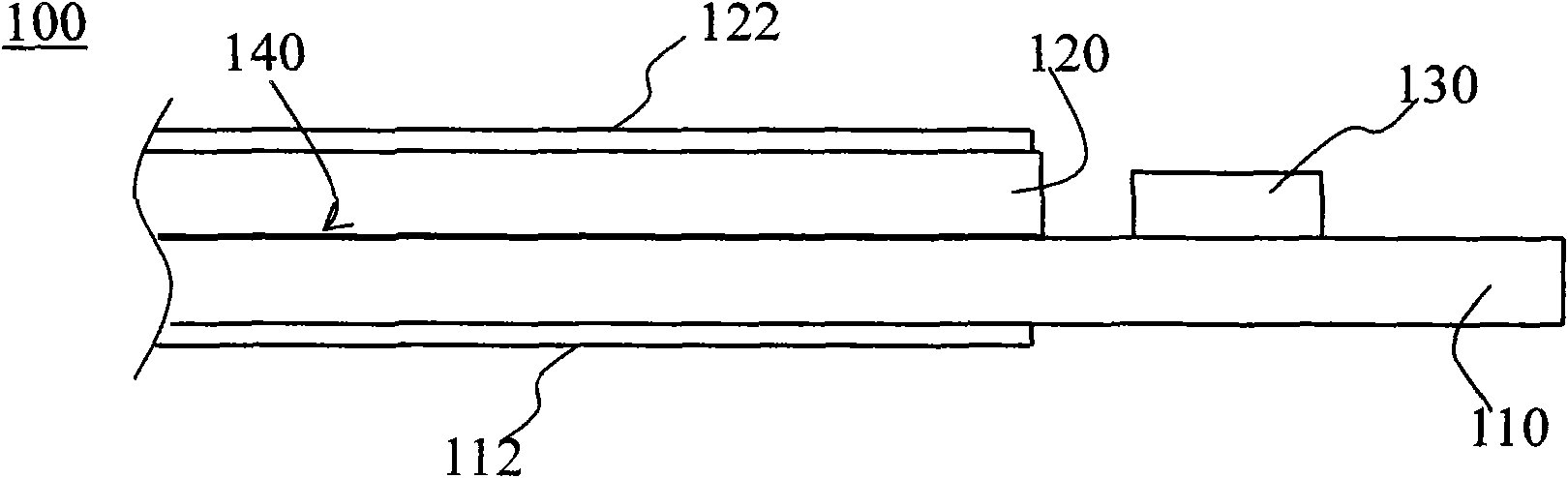
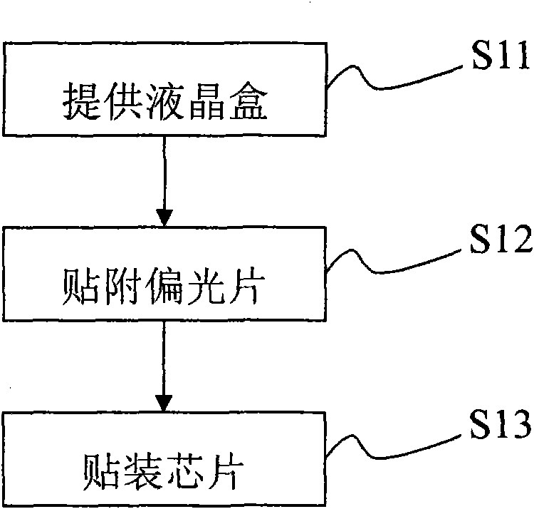
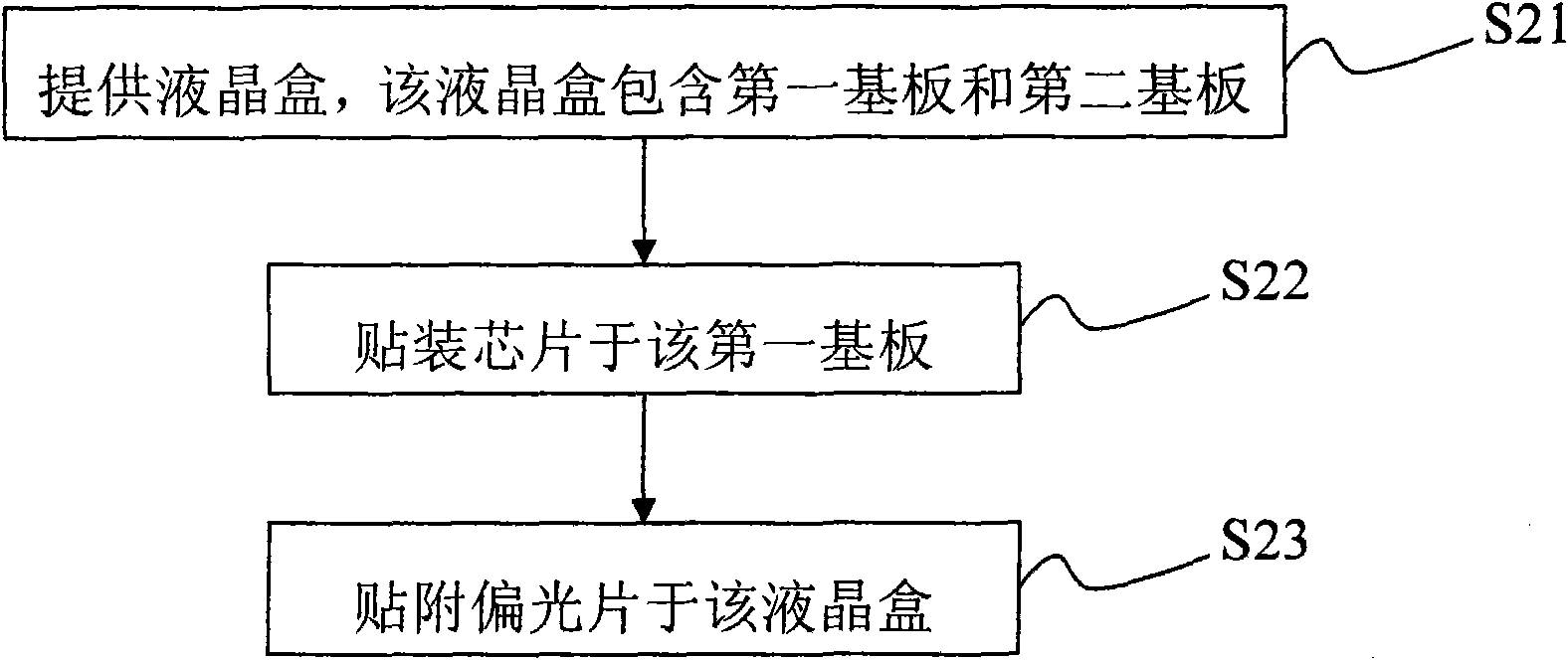
[0018] See image 3 , image 3 It is a flowchart of a method for manufacturing a liquid crystal panel according to an embodiment of the present invention. The manufacturing method of the liquid crystal panel includes the following steps. S21, providing a liquid crystal cell, where the liquid crystal cell includes a first substrate and a second substrate. S22, mounting chips on the first substrate. S23, attaching a polarizer to the liquid crystal cell. In one embodiment, the first substrate has a thin film transistor array, and the second substrate has a color filter layer. Before the step of mounting the chip on the first substrate, other steps may also be included, such as laser cutting, cleaning the end face of the liquid crystal cell, and the like. After the ...


PUM


Abstract

The invention discloses an LCD panel manufacturing method, comprising the following steps: providing an LCD box which comprises a first base plate and a second base plate; sticking a chip on the first base plate; and attaching a polaroid in the LCD box. The invention can greatly promote anti-compressive strength without influencing capacity and yield.

Description

technical field [0001] The present invention relates to a method for manufacturing a liquid crystal panel, in particular to a method for manufacturing a liquid crystal panel that can increase the squeeze strength of the panel. Background technique [0002] Liquid crystal display devices have the advantages of high image quality, small size, light weight, low voltage drive, and low power consumption. Therefore, they have been widely used in various electronic products such as TVs, telephones, cameras, notebook computers, and desktop monitors. The mainstream of flat panel displays. [0003] A liquid crystal panel is one of the key components of a liquid crystal display device. See figure 1 , figure 1 It is a schematic structural diagram of a liquid crystal panel 100 in the prior art. The liquid crystal panel 100 comprises a liquid crystal box (cell) made up of a first substrate 110 and a second substrate 120, which is filled with a liquid crystal 140, the first substrate 1...

Claims


Application Information

Patent Timeline
Patent Type & Authority Applications(China)
IPC IPC(8): G02F1/13G02F1/1333
Inventor 蔡水源银建
Owner AU OPTRONICS (XIAMEN) CORP
Why Eureka
Try Eureka