

Liquid crystal alignment process
A liquid crystal alignment and liquid crystal technology, applied in nonlinear optics, instruments, optics, etc., can solve problems such as pollution, high cost, and waste, and achieve the effects of reducing production costs, improving efficiency, and reducing time costs
- Summary
- Abstract
- Description
- Claims
- Application Information
AI Technical Summary
Problems solved by technology
Method used
Image

Examples
Embodiment Construction
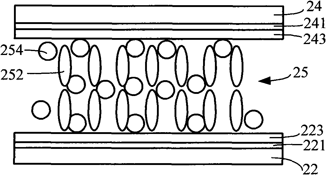
[0030] see Figure 3A to Figure 3D , which shows a flow chart of the liquid crystal alignment process implemented according to the present invention. Such as Figure 3AAs shown, a first substrate 32 and a second substrate 34 parallel to the first substrate 32 are provided, the first substrate 32 can be a thin film transistor array substrate (TFT array substrate), and the second substrate 34 can be an opposing substrate, Or a color filter substrate (color filter substrate, CF substrate). A first conductive layer 321 and a second conductive layer 341 are disposed on opposite surfaces of the first substrate 22 and the second substrate 24 respectively, and the conductive layers 321 and 341 can be transparent ITO film. A liquid crystal accommodating space 35 is formed between the two substrates 32 and 34 , more specifically, it is located between the two conductive layers 321 and 341 .
[0031] Such as Figure 3A As shown, a liquid crystal composition 350 is poured into the liq...
PUM
 Abstract
Description
Claims
Application Information