

Optical filter for display, method for manufacturing the same, and display and plasma display panel equipped with optical filter for display
A technology of optical filter and manufacturing method, applied in the direction of optics, optical components, nonlinear optics, etc., to achieve the effect of easy grounding and suppression of peeling damage
- Summary
- Abstract
- Description
- Claims
- Application Information
AI Technical Summary
Problems solved by technology
Method used
Image

Examples
Embodiment 1
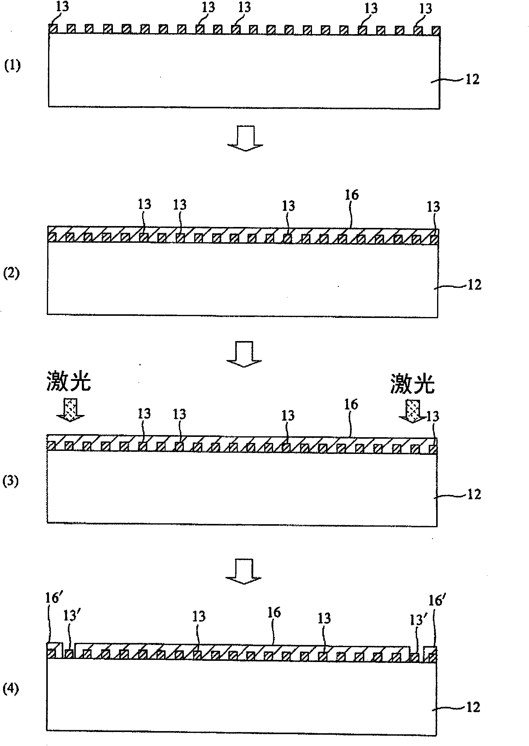
[0197]
[0198] (1) Formation of mesh metal conductive layer
[0199] Polyethylene terephthalate film (width: 600mm, length 100m) with a 100μm-thick long polyethylene terephthalate film (width: 600mm, length 100m) having an easy-adhesive layer (polyester polyurethane; thickness 20nm) on the surface is printed with dots of polyester 20% aqueous solution of vinyl alcohol. The size of one dot is a square shape with a side length of 234 μm, the interval between dots is 20 μm, and the dots are arranged in a square lattice. The printing thickness was about 5 μm after drying.
[0200] Copper with an average film thickness of 4 μm was vacuum-deposited thereon. Then immerse it in water at normal temperature, wipe it with a sponge, dissolve and remove some of the dots, then wash it with water, and form a mesh conductive layer on the entire surface of the polyethylene film after drying (refer to figure 1 (1)).
[0201] The conductive layer on the surface of the film is a square gr...
PUM
| Property | Measurement | Unit |
|---|---|---|
| diameter | aaaaa | aaaaa |
| wavelength | aaaaa | aaaaa |
| particle size | aaaaa | aaaaa |
Abstract
Description
Claims
Application Information