

Anti-radiation EEPROM memory array structure
A storage array, radiation-resistant technology, applied in electrical components, electric solid-state devices, circuits, etc., can solve the problem that the EEPROM memory cell array structure does not have application value, etc., and achieve the effect of improving radiation resistance.
- Summary
- Abstract
- Description
- Claims
- Application Information
AI Technical Summary
Problems solved by technology
Method used
Image

Examples
Embodiment Construction
[0014] Below in conjunction with accompanying drawing and embodiment the technical scheme of invention is described in detail:
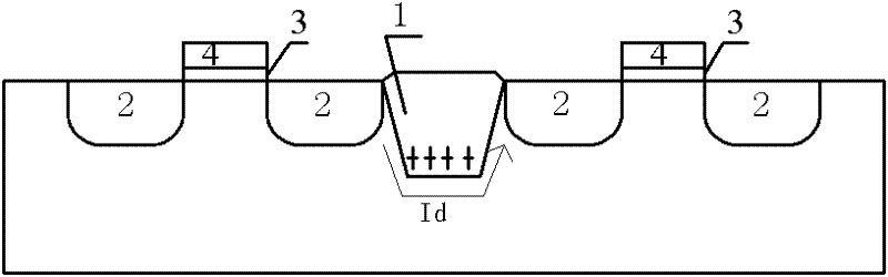
[0015] According to the leakage principle of field oxygen isolation, such as figure 2 In the shown structure, a polycrystalline ring is added on the periphery of each memory cell, and the polycrystalline ring forms an HVNMOS isolation transistor with the N-type active region of the adjacent cell.
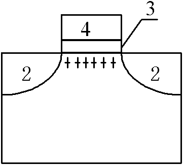
[0016] figure 2 In the shown structure, an isolation structure of an HVNMOS transistor is formed between the units. The working process and working principle of the structure are as follows: image 3 As shown, 2 is the respective N-type active regions of two adjacent memory cells, 3 is the gate oxide layer, and 4 is the polysilicon gate (that is, the gate of the HVNMOS isolation transistor). and figure 1 In contrast, there is no field oxygen region between the cells, and the active area between the cells forms the active area of the HVNMOS isolatio...
PUM
 Abstract
Description
Claims
Application Information