Method and structure for eliminating offset voltage of operational amplifier by using lining bias effect

A technology of bias effect and offset voltage, applied in improving amplifiers to reduce temperature/power supply voltage changes, differential amplifiers, DC-coupled DC amplifiers, etc., can solve problems such as increasing parasitic capacitance, reducing circuit speed, and unable to eradicate offset voltage

Active Publication Date: 2013-01-30
杭州思泰微电子有限公司
View PDF0 Cites 0 Cited by
  • Summary
  • Abstract
  • Description
  • Claims
  • Application Information

AI Technical Summary

Problems solved by technology

It can only reduce the offset voltage of the op amp to a certain extent, but it cannot eradicate the offset voltage of the op amp
Complicated drawing will make the connection complicated, increase parasitic capacitance, and reduce the speed of the circuit;
[0008] 3) Use two-phase clock elimination, which is commonly used in discrete switched capacitor signals and cannot be used in continuous signals, which limits the application occasions;
Adds redundant circuits, increases parasitic capacitance, and reduces circuit speed

Method used


Image

  • Method and structure for eliminating offset voltage of operational amplifier by using lining bias effect
  • Method and structure for eliminating offset voltage of operational amplifier by using lining bias effect
  • Method and structure for eliminating offset voltage of operational amplifier by using lining bias effect

Examples


Embodiment Construction

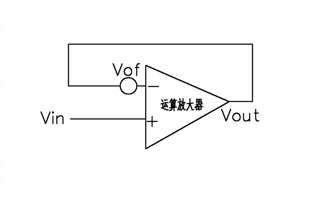
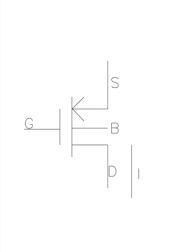
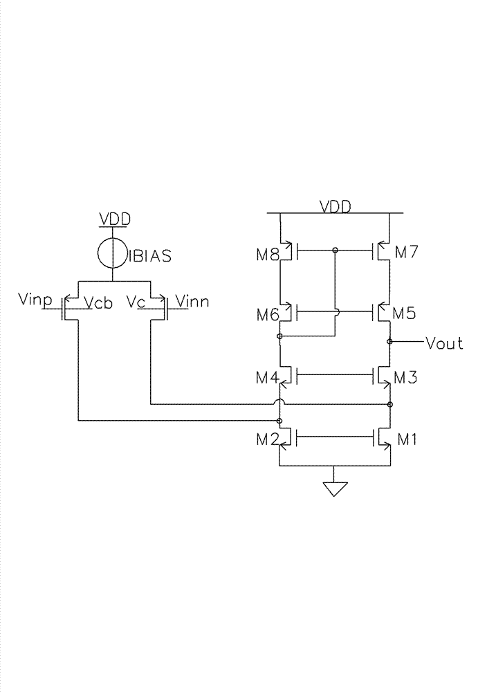
[0025] A method of eliminating the offset voltage of an op amp by using the substrate bias effect, see Figure 4 , Figure 5 , which includes an operational amplifier. When correcting, the two input terminals of the operational amplifier are grounded. Among the two PMOS transistors of the operational amplifier, the substrate voltage of one PMOS transistor is connected to the fixed voltage Vc, and the substrate voltage of the other PMOS transistor can be connected to Variable voltage Vcb, the output terminal Vout of the operational amplifier is connected to the negative pole of the comparator, the positive pole of the comparator is connected to the reference voltage V, and the output of the comparator is connected to the subtractor. In a single clock cycle T, the positive pole of the comparator is smaller than the negative pole. The output is 0, the subtractor subtracts 1, and the value corresponding to the output of the subtractor controls the value of the variable voltage Vcb...


PUM


Abstract

The invention provides a method and a structure for eliminating offset voltage of an operational amplifier by using a lining bias effect, which can effectively eliminate the offset voltage of the operational amplifier without causing extra capacitance or influencing the speed of the operational amplifier. The structure is characterized in that: during correction, two input ends of the operational amplifier are grounded; in two P-channel metal oxide semiconductor (PMOS) transistors of the operational amplifier, the substrate voltage of one PMOS transistor is connected with a fixed voltage Vc and the substrate voltage of the other PMOS transistor is connected with a variable voltage Vcb; the output end Vout of the operational amplifier is connected with the negative electrode of a comparator; the positive electrode of the comparator is connected with a reference voltage V; the output of the comparator is connected with a subtractor; in a single clock period T, the positive voltage value of the comparator is less than the negative voltage value; the output is 0, 1 is subtracted by the subtractor, the numerical value of the variable voltage Vcb is controlled by controlling a voltage type digital-analog converter for the corresponding output numerical value, and further the Vout is reduced until the Vout is less than V; at the time, the output of the comparator is 1, and the subtractor stops subtraction; and thus, the numerical value of the voltage Vcb of the voltage type digital-analog converter is kept unchanged.

Description

technical field [0001] The invention relates to the technical field of operational amplifiers under the CMOS process, specifically a method for eliminating the offset voltage of the operational amplifier by using the substrate bias effect, and the invention also provides a structure using the method. Background technique [0002] The development of CMOS technology is advancing by leaps and bounds. With its low price, low power consumption and high integration, it has become the most important chip production technology today. Products in various application fields based on CMOS technology emerge in an endless stream. As a basic module of the electronic system, the operational amplifier has a wide range of applications, and its own performance greatly affects the performance of the system. [0003] In an ideal op amp, each device is symmetrical, but in the CMOS production process, due to fluctuations in the manufacturing process, there will be differences between compone...

Claims


Application Information

Patent Timeline
IPC IPC(8): H03F1/30H03F3/45
Inventor 吴明远应祖金黄海滨
Owner 杭州思泰微电子有限公司
Why Eureka
Try Eureka