Apparatus for array test with cleaner units

A technology for array testing and cleaning cells, applied in measurement devices, cleaning methods and utensils, cleaning methods using gas flow, etc., can solve problems such as reducing test reliability and accuracy, foreign matter introduction, etc

Inactive Publication Date: 2011-03-23
TOP ENG CO LTD
View PDF8 Cites 14 Cited by
  • Summary
  • Abstract
  • Description
  • Claims
  • Application Information

AI Technical Summary

Problems solved by technology

[0008] However, conventional array substrates have a problem that foreign matter may be attached to the surface of the substrate during the process of transferring or testing the substrate.
This foreign matter can reduce the reliability and accuracy of any test

Method used


Image

  • Apparatus for array test with cleaner units
  • Apparatus for array test with cleaner units
  • Apparatus for array test with cleaner units

Examples


Embodiment Construction

[0034] The following detailed description is intended to assist the reader in gaining a comprehensive understanding of the methods, apparatus and / or systems presented herein. Various changes, modifications, and equivalents to the systems, devices, and / or methods described herein will be apparent to those of ordinary skill in the art. Descriptions of well-known functions and constructions are omitted for conciseness.

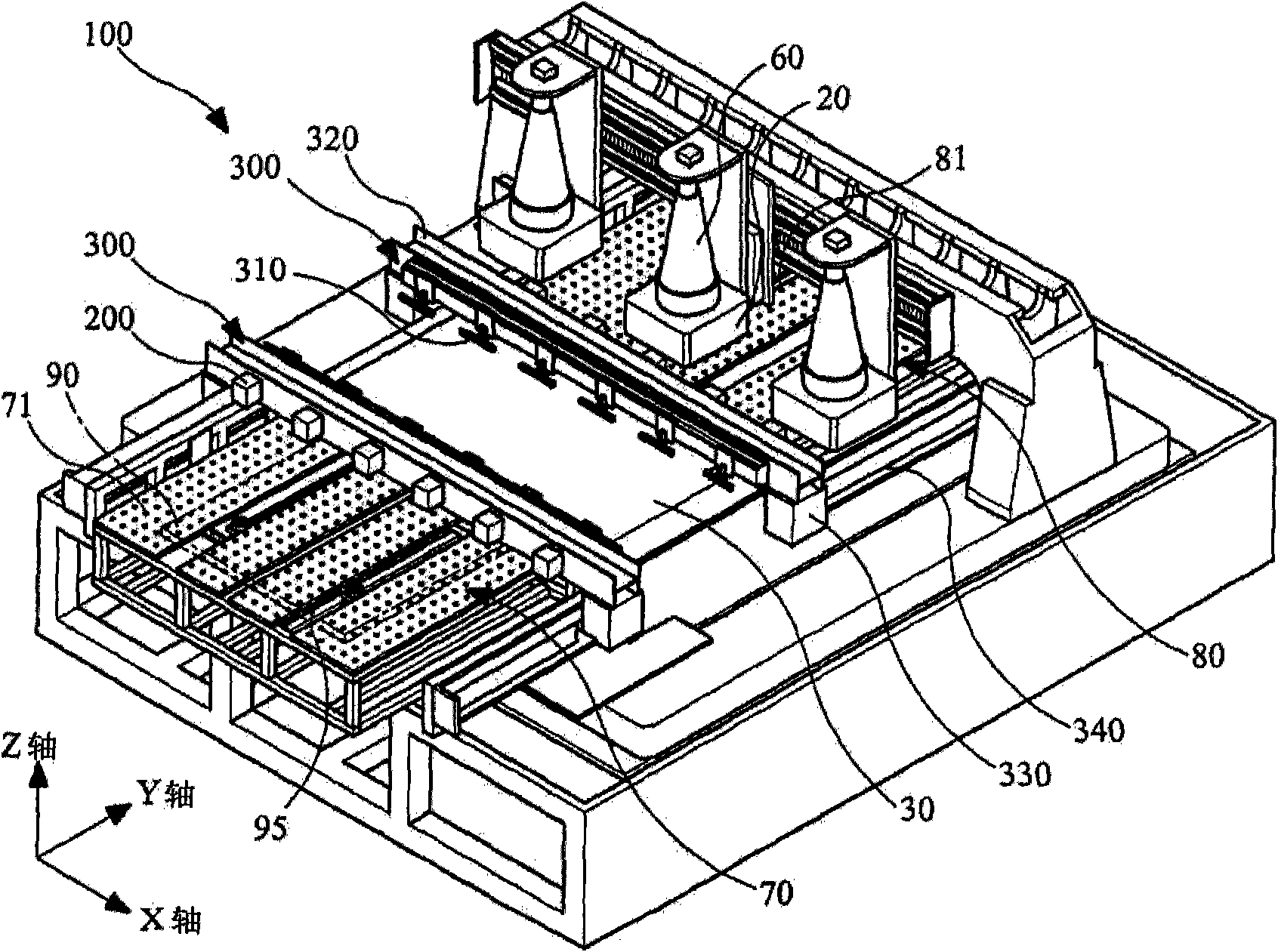
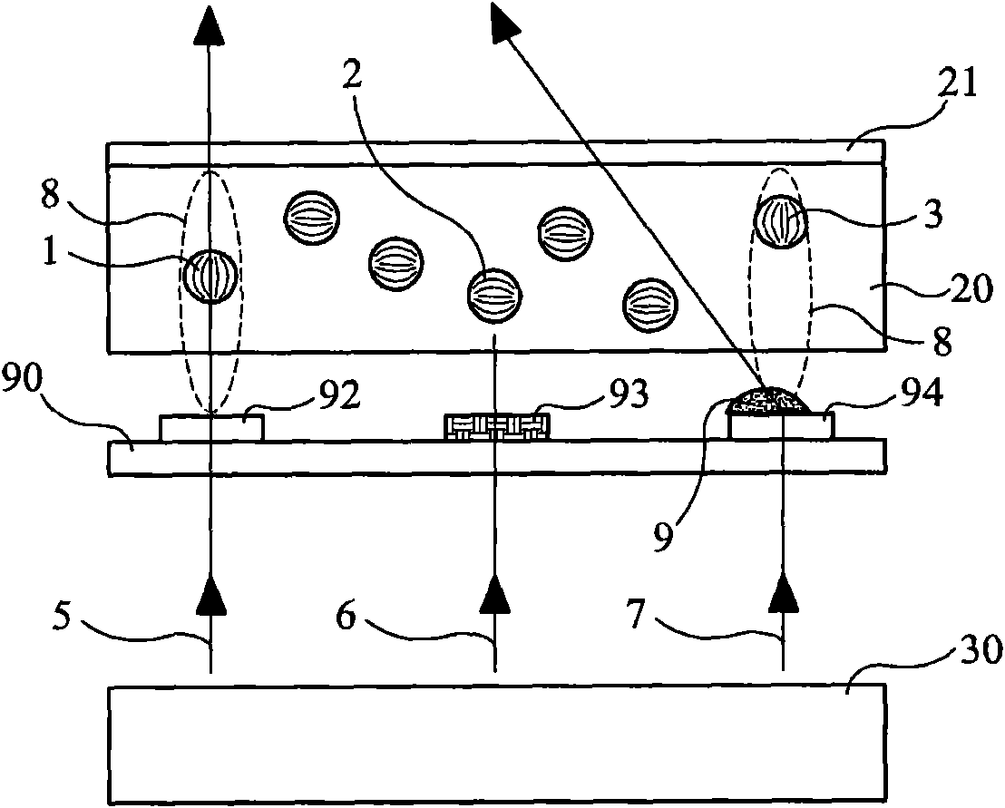
[0035] The array testing device includes a probe assembly. The probe assembly applies a voltage to the electrodes formed on the substrate to test the electrode array formed on the substrate.

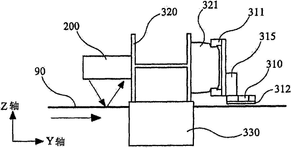
[0036] Specifically, the probe assembly includes a cleaning unit. A cleaning unit equipped for the probe assembly removes foreign matter from the substrate. Therefore, it is possible to effectively remove fine foreign matter that may be generated during transfer of the substrate or driving of the probe assembly.

[0037] Hereinafter, the technical structure of the array...


PUM


Abstract

The present invention provides an apparatus for array test, which is used for detecting the defect in an electrode that is formed in a display substrate. A probe assembly comprises a probe rod and a probe frame. The probe rod comprises probe pins which are used for applying a voltage to the electrode formed on the display substrate. The probe frame is connected with the probe rods so that the probe rods can move in one direction relatively to the substrate. The probe frame is connected with cleaner units. Therefore, through the cleaning units, the foreign matter which is additionally generated possibly in substrate transferring or probe assembly operation period in the array test process can be removed, thereby improving test reliability.

Description

[0001] Cross References to Related Applications [0002] This application claims the priority benefit of Korean Patent Application No. 10-2009-0071427 filed on Aug. 3, 2009, the disclosure of which is hereby incorporated by reference in its entirety for various purposes. technical field [0003] The following description relates to an apparatus for testing a display, in particular, an array testing apparatus for detecting electrical defects of electrodes formed on a display substrate. Background technique [0004] Recently, display panels have become increasingly slimmer, and current flat panel displays include types such as liquid crystal displays, plasma display panels (PDPs), and organic light emitting diodes (OLEDs). A general thin film transistor (TFT) LCD includes: a TFT substrate, a color substrate on which a color filter and a common electrode are formed and arranged to face the TFT substrate, a liquid crystal arranged between the TFT substrate and the color substrat...

Claims


Application Information

Patent Timeline
Patent Type & Authority Applications(China)
IPC IPC(8): G09G3/00G01R31/00G01R1/067B08B5/02B08B5/04B08B15/04B08B5/00B08B7/02B08B7/04B08B7/00B03C1/02
CPCG01R1/073G01R31/2836G01R31/2879G01R31/2886H01L21/02046
Inventor 朴廷喜
Owner TOP ENG CO LTD
Why Eureka
Try Eureka