Method of fabricating and encapsulating mems devices

A technology for encapsulating films and microstructures, which is applied in the direction of assembling microstructure devices, microstructure devices, and manufacturing microstructure devices, etc.

Inactive Publication Date: 2011-04-06
SHANGHAI LEXVU OPTO MICROELECTRONICS TECH
View PDF8 Cites 25 Cited by
  • Summary
  • Abstract
  • Description
  • Claims
  • Application Information

AI Technical Summary

Problems solved by technology

This is something that the existing technology has not successfully solved so far.

Method used


Image

  • Method of fabricating and encapsulating mems devices
  • Method of fabricating and encapsulating mems devices
  • Method of fabricating and encapsulating mems devices

Examples


Embodiment Construction

[0026] The drawings used for illustration are not strictly to scale, but generally illustrate the framework and principles of the invention. In the following description, reference is made to the accompanying drawings which form a part hereof, showing by way of illustration preferred embodiments of the invention. It is to be understood that other embodiments may be utilized and structural changes may be made without departing from the scope of the present invention.

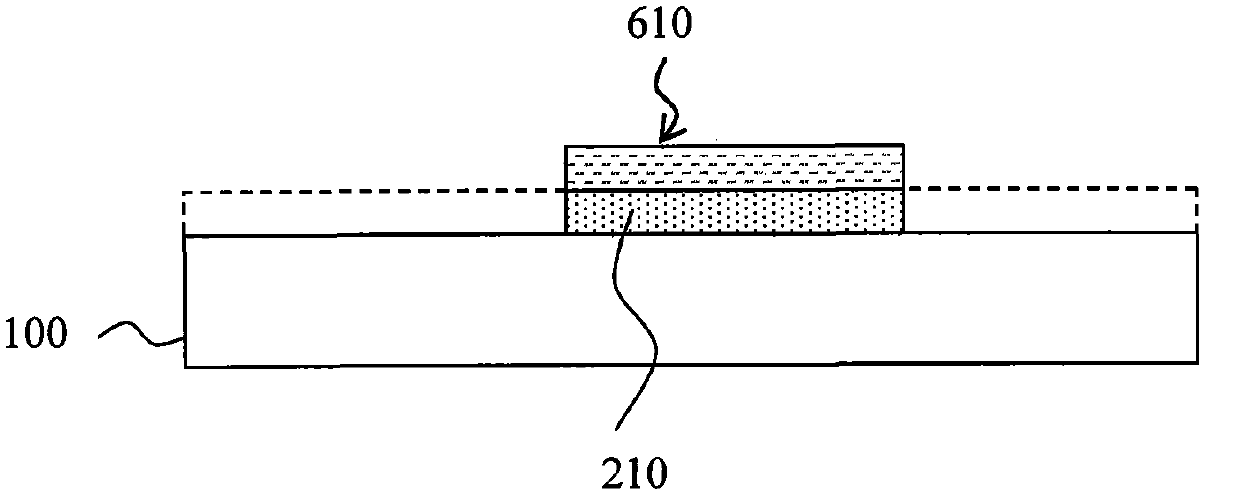
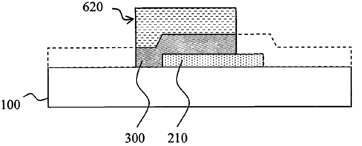
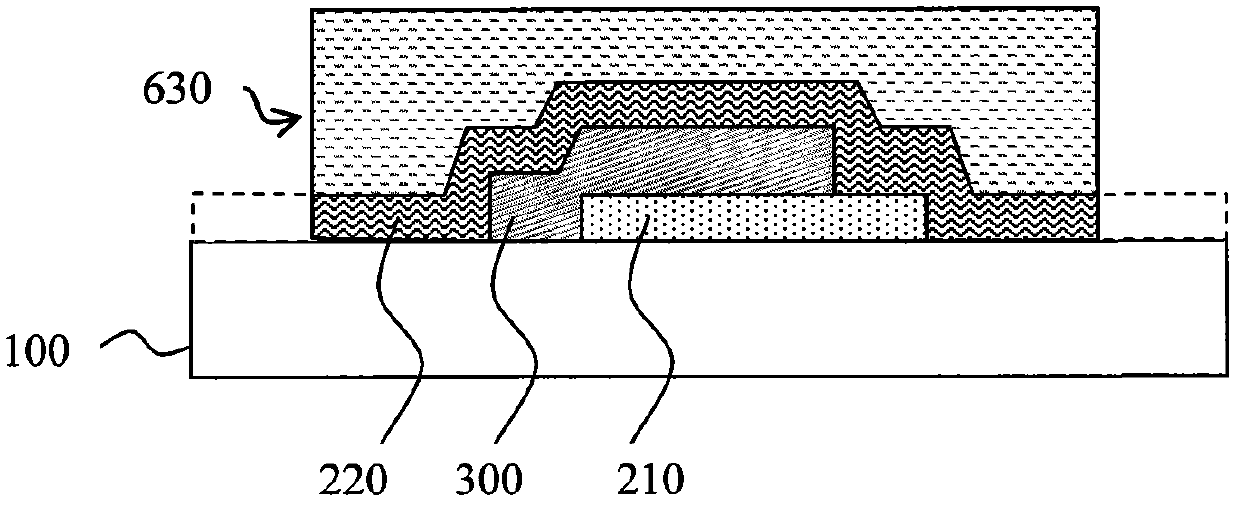
[0027] Figure 1a , 1b , 1c, 1d, 1e, 1f show in cross-sectional views the use of the first sacrificial carbon film 210 and the second sacrificial carbon film 220 as double sacrificial layers to assemble and package the structural element 300 suspended on the substrate 100 in sequential basic steps A basic embodiment of the method is disclosed. like Figure 1a As shown, the steps of depositing the first sacrificial carbon film 210 are as follows: placing the substrate 100 in the reactor chamber, introducing a ca...


PUM


Abstract

A method of fabricating and encapsulating MEMS devices is disclosed, using least two carbon films as the dual sacrificial layers sandwiching a MEMS structural film which is anchored onto a substrate and covered by an encapsulating film containing a plurality of thru-film sacrificial release holes. The dual sacrificial carbon films are selectively removed via plasma-enhanced oxygen or nitrogen ashing through the thru-film sacrificial release holes for releasing the MEMS structural film inside a cavity formed between the encapsulating film and the substrate. The thru-film sacrificial release holes, preferably with a relative high asperity ratio, are then sealed off by depositing a hole-sealing film in a physical vapor deposition process or a chemical vapor deposition process or combination.

Description

[0001] Cross References to Related Applications [0002] This application claims priority to U.S. Provisional Application No. 61 / 238,440, entitled "Methods of Assembling and Encapsulating Micro-Electro-Mechanical Systems Devices," filed August 31, 2009, the entire contents of which are hereby incorporated by reference . technical field [0003] The present invention relates to a method for processing suspension structural elements in a microelectromechanical system (hereinafter referred to as "MEMS") device, and in particular to a method for assembling and packaging a suspension in a MEMS device in a chamber above a solid substrate using a double sacrificial carbon film. Set structural elements. Background technique [0004] MEMS include integrated microdevices, such as mechanical, optical, and heat-sensitive components, formed on a substrate made of a single layer or composite layers of solid-state materials. MEMS are preferably assembled using existing wafer batch proces...

Claims


Application Information

Patent Timeline
Patent Type & Authority Applications(China)
IPC IPC(8): B81C1/00
CPCB81C2203/0145B81C2203/0136B81C1/00333
Inventor 河·H·黄
Owner SHANGHAI LEXVU OPTO MICROELECTRONICS TECH
Why Eureka
Try Eureka