Light guide member, planar light source device provided with the light guide member, and display apparatus using the planar light source device
A technology of light guide components and display equipment, which is applied to the parts, light sources, electric light sources and other directions of lighting devices, can solve the problems of increased backlight thickness and high brightness, and achieve uniform brightness distribution, high brightness, and improved light utilization. Effect
- Summary
- Abstract
- Description
- Claims
- Application Information
AI Technical Summary
Problems solved by technology
Method used
Image

Examples
Embodiment 1
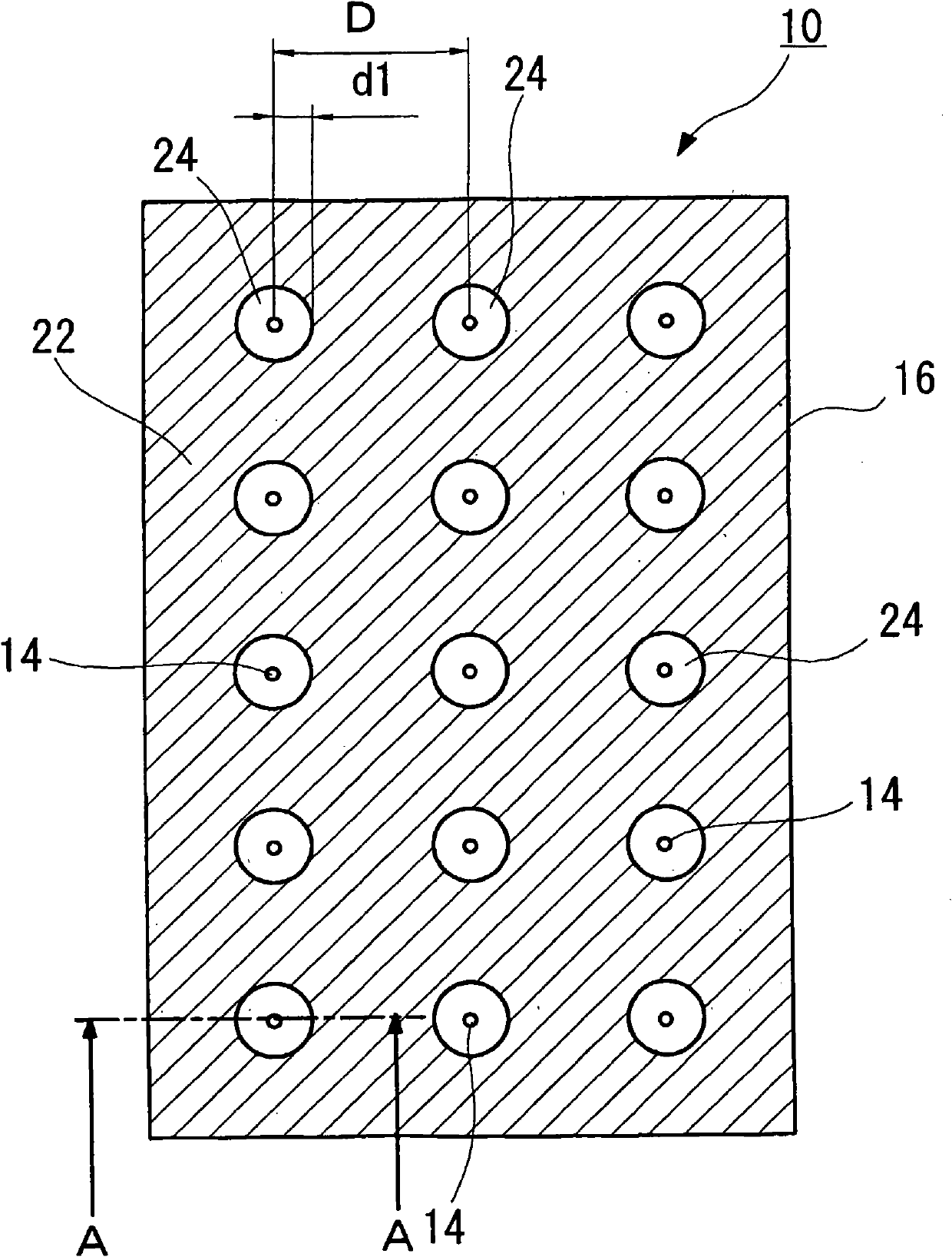
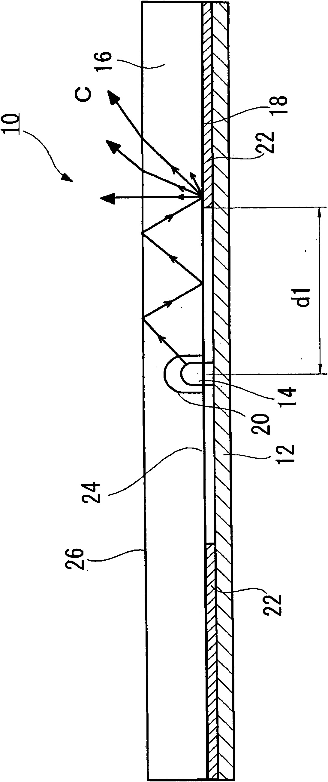
[0221] Unit light-emitting devices such as figure 2 It is shown that the light emitting device mounting substrate 12 is placed in an array pattern with a width of 115 mm x a length of 135 mm, in which 1W red, green, and blue LED chips are combined to form the light emitting device 14.
[0222] A transparent plate made of acrylic resin with a width of 115 mm x a length of 135 mm and a thickness of 3 mm is used as the light guide member 16.
[0223] A hemispherical recess 20 for a light emitting device with a radius of 2.5 mm is formed on the bottom surface 18 of the light guide member 16 directly above the center of each light emitting device 14.
[0224] A white paint made of acrylic resin containing 50% of titanium dioxide (solid matter only) was coated on the bottom surface 18 of the light guide member 16 by spray coating so that the film thickness was 100 m, thereby forming the light reflecting portion 22.
[0225] In this case, the light-reflecting portion 22 is formed in a region...
Embodiment 2
[0232] According to the invention such as Figure 19 The illustrated surface light source device 10 is obtained in a manner similar to Embodiment 1, except for the following aspects.
[0233] More specifically, such as Picture 8 with Picture 9 As shown, at a position corresponding to the light emitting device 14 on the upper surface of the light guide member 16, that is, at a position directly above the light emitting device 14, a circular semi-transmissive portion 32 is further formed.
[0234] A white paint made of acrylic resin containing 50% of titanium dioxide (solid matter only) is spray-coated on the upper surface area of the light guide member so that the film thickness is 20 μm, thereby forming a semi-transmissive portion 32, wherein The distance d2 from the light emitting device 14 to the outer peripheral edge of the semi-transmissive portion 32 is 5 mm.
[0235] Thus, next, similarly to Example 1, the relative brightness was measured at a distance of 0.5 mm from the po...
Embodiment 3
[0238] According to the invention such as Figure 20 The illustrated surface light source device 10 is obtained in a manner similar to Embodiment 1, except for the following aspects.
[0239] More specifically, the semi-transmissive portion 11 is formed on the concave surface of the concave portion 20 for the light emitting device.
[0240] A white paint made of acrylic resin containing 50% of titanium dioxide was applied by spraying so that the film thickness was 20 μm, thereby forming the semi-transmissive portion 11.
[0241] The range in which the translucent portion 11 is formed, that is, the projection distance d3 from the center of the light emitting device 14 to the outer peripheral edge of the translucent portion 11 is about 1.8 mm, such that Figure 20 The red, green and blue LED chips shown are basically covered.
[0242] Almost the entire surface of the bottom surface 18 of the light guide member 16 is coated with a white paint made of acrylic resin containing 50% of titani...
PUM
 Abstract
Description
Claims
Application Information
 - R&D Engineer
- R&D Manager
- IP Professional
- Industry Leading Data Capabilities
- Powerful AI technology
- Patent DNA Extraction
Browse by: Latest US Patents, China's latest patents, Technical Efficacy Thesaurus, Application Domain, Technology Topic.
© 2024 PatSnap. All rights reserved.Legal|Privacy policy|Modern Slavery Act Transparency Statement|Sitemap