Method for preparing transmission electron microscope sample

An electron microscope and sample technology, applied in the field of semiconductor and material analysis, can solve the problems of reducing sample preparation efficiency, affecting observation effect, and inability to clearly image, etc., and achieve the effect of improving preparation efficiency and observation effect

Inactive Publication Date: 2011-04-20
SEMICON MFG INT (SHANGHAI) CORP
View PDF1 Cites 53 Cited by
  • Summary
  • Abstract
  • Description
  • Claims
  • Application Information

AI Technical Summary

Problems solved by technology

However, if image 3 As shown, if the failure region 103 also has an extended structure from the bottom surface of the sample to the surface or a multilayer stacked structure ( image 3 Taking the multilayer stack structure as an example, the multilayer stack structure is stacked layers 110, 109, 108, 107, 106 from the surface to the bottom surface respectively), in order to observe a complete extended structure or a multilayer stack structure, the pit 101 and 102 must be greater than or equal to the length of the extension structure or the thickness of the stacked structure. In order to obtain a larger depth, the length and width of the pits 101, 102 also need to be correspondingly larger, making the grinding process time-consuming Longer, that is, the grinding amount of the focused ion beam is positively correlat...

Method used


Image

  • Method for preparing transmission electron microscope sample
  • Method for preparing transmission electron microscope sample
  • Method for preparing transmission electron microscope sample

Examples


Embodiment Construction

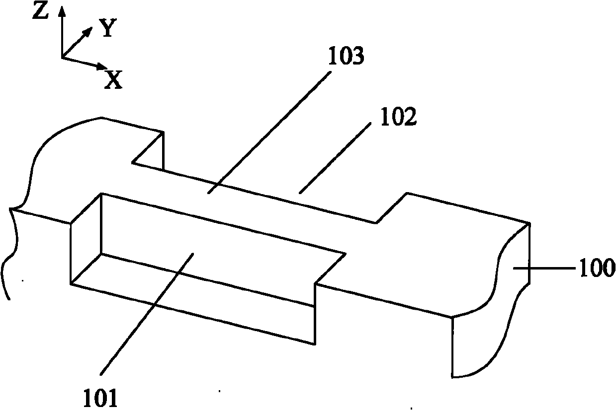
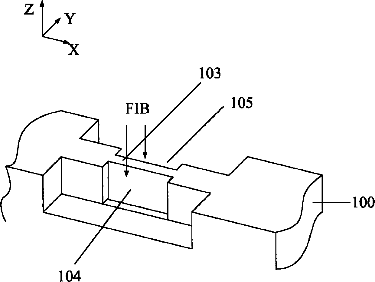
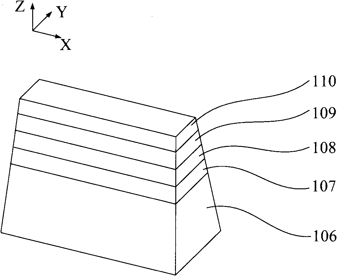
[0033] The invention provides a method for preparing a transmission electron microscope sample. First, the area to be observed is marked, and then the sample is ground along a direction perpendicular to the elongation direction of the elongated structure or the stacking direction of the stacked structure, and then Forming pits on both sides of the area to be observed on the grinding surface and thinning the area to be observed along the pits, avoiding the positive correlation between the amount of grinding and the length of the extended structure or the thickness of the multilayer stacked structure , so that the area to be observed can be clearly imaged under the transmission electron microscope, which improves the preparation efficiency and observation effect.

[0034] During the preparation process, a protective cover is further installed on the surface of the sample, which prevents the sample from being damaged during the grinding process, and also avoids the problem that it...


PUM

PropertyMeasurementUnit
Thicknessaaaaaaaaaa

Abstract

The invention discloses a method for preparing a transmission electron microscope sample. The method comprises the following steps of: providing a sample with length, width and thickness, wherein at least one elongation structure or multi-layer stack structure along the thickness direction is formed in a region to be observed of the sample; marking the region to be observed of the sample; grinding the sample along a direction which is perpendicular to the elongation direction of the elongation structure or the stacking direction of the stack structure until the mark is exposed; forming a concave pit on the two sides of the region to be observed on a grinding surface respectively; thinning the sample part of the marked region along the concave pit to a specific thickness; and separating and taking the thinned sample part at the region to be observed out. By the method, the preparation efficiency and the observation effect are improved, a protective cover is further assembled on the surface of the sample during the preparation, the sample is prevented from being damaged during the grinding, and the problem that the sample at the region to be observed can easily fall off and bounce out after the preparation is finished is also prevented.

Description

technical field [0001] The invention relates to the field of semiconductor technology and the field of material analysis technology, in particular to a method for preparing a transmission electron microscope sample. Background technique [0002] With the development of semiconductor technology, the complexity and integration of integrated circuits continue to increase, and the number of devices integrated on a single chip has reached hundreds of millions or even billions. To meet the challenges, such as optical microscope (OM) and scanning electron microscope (SEM) can no longer meet the requirements. Due to the high resolution of Transmission Electron Microscope (TEM, Transmission Electron Microscope) can observe the internal structure of the thin film region. Therefore, with the continuous improvement of the semiconductor process level, especially after entering the 130nm process, the Transmission Electron Microscope has become an integrated method for observation and anal...

Claims


Application Information

Patent Timeline
IPC IPC(8): G01N1/28G01N1/32
Inventor 庞凌华段淑卿王玉科杨卫明李剑
Owner SEMICON MFG INT (SHANGHAI) CORP
Why Eureka
Try Eureka