Method for reducing reflection power in plasma etching

A technology of reflected power and plasma, which is applied in the direction of plasma, semiconductor/solid-state device manufacturing, discharge tube, etc., can solve problems such as short circuit or open circuit of logic circuit, lower product yield, polymer bombardment, etc., to reduce reflected power , the effect of improving the yield rate

Active Publication Date: 2012-07-25
SEMICON MFG INT (SHANGHAI) CORP
View PDF0 Cites 0 Cited by
  • Summary
  • Abstract
  • Description
  • Claims
  • Application Information

AI Technical Summary

Problems solved by technology

Due to the great change in the environmental conditions in the above-mentioned reaction chamber, the components of the reaction chamber itself cannot be adjusted accordingly (turning) and feedback, resulting in increased reflected power
When the reflected power is too large, the polymer on the reaction chamber may be bombarded and fall on the wafer, causing the logic circuit on the semiconductor device to be short-circuited or disconnected, thereby causing the product to be scrapped and greatly reducing the quality of the product. yield

Method used


Image

  • Method for reducing reflection power in plasma etching
  • Method for reducing reflection power in plasma etching
  • Method for reducing reflection power in plasma etching

Examples


Embodiment Construction

[0050] In order to make the object, technical solution and advantages of the present invention more clear, the present invention will be further described in detail by giving specific embodiments and referring to the accompanying drawings.

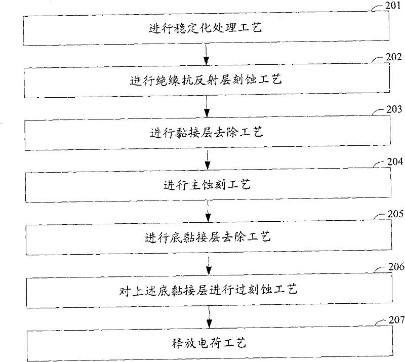
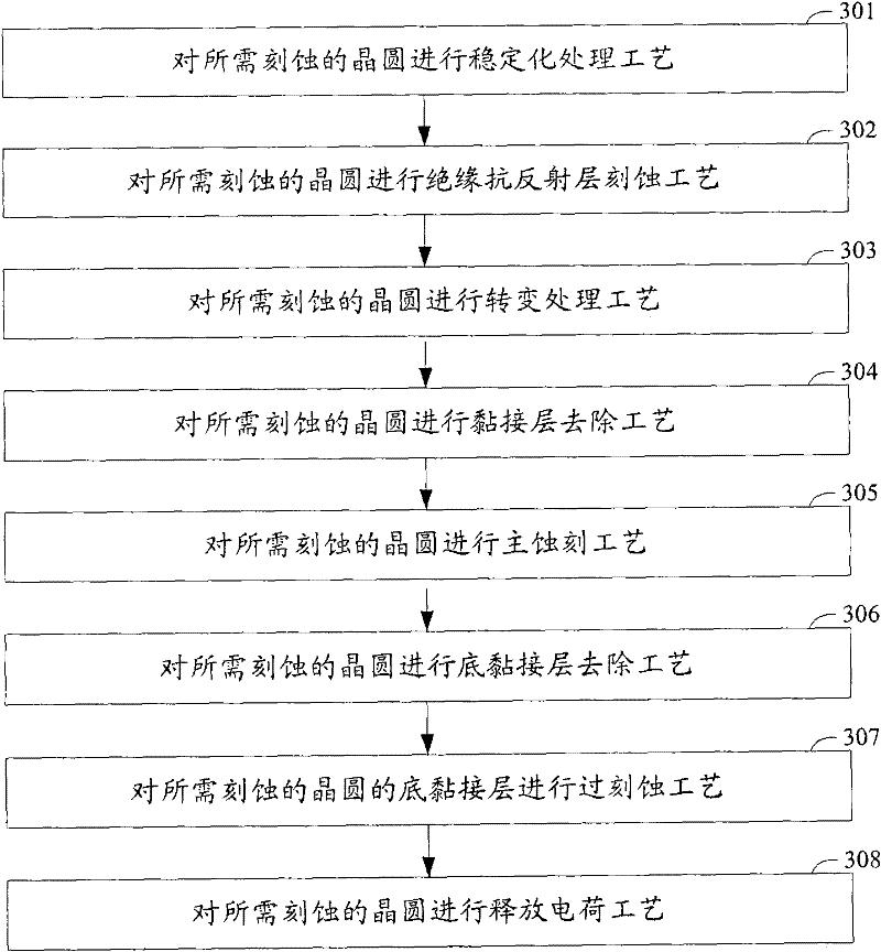
[0051] The invention provides a method for reducing the reflected power in plasma etching, in which method, the wafer to be etched will be subjected to a stabilization treatment process, an insulating anti-reflection layer etching process, and transformation ( transition) treatment process, adhesive layer removal process, main etching process, bottom adhesive layer removal process, over-etching process and charge release process to complete the etching of the metal layer of the wafer. Wherein, a conversion treatment process is added between the insulating anti-reflection layer etching process and the adhesive layer removal process. In the conversion process, the source power is first reduced to a preset source power value, and the reduced ...


PUM


Abstract

The invention discloses a method for reducing reflection power in plasma etching. The method comprises the following steps of: performing a stabilization process, performing a transformation process, an insulating antireflection layer etching process, an adhesive layer removing process, a main etching process, a bottom adhesive layer removing process, an over-etching process and a charge releasing process on a wafer to be etched in turn; and etching a metal layer of the wafer. By the method, the reflection power can be effectively reduced, and the yield of a product is improved.

Description

technical field [0001] The invention relates to the field of semiconductor manufacturing, in particular to a method for reducing reflected power in plasma etching. Background technique [0002] In the manufacturing process of large-scale integrated circuits (ICs), with the continuous increase of the integration level of integrated circuits, the area of ​​semiconductor elements is gradually reduced, and the design line width of integrated circuits is also getting smaller and smaller. In the prior art, an etching method is generally used to form an extremely fine-sized circuit structure on a semiconductor element, and plasma etching is one of the most commonly used etching methods. [0003] In the plasma etching, a group of high-power radio frequency excitation power sources are generally used to make the etching gas in the reaction chamber generate a glow discharge under the action of a high-frequency electric field (frequency is usually 13.56 MHz), so that the etching gas T...

Claims


Application Information

Patent Timeline
Patent Type & Authority Patents(China)
IPC IPC(8): H01L21/00H01J37/32H05H1/46
Inventor 张松山孙长勇
Owner SEMICON MFG INT (SHANGHAI) CORP
Why Eureka
Try Eureka