Vacuum processing apparatus

a vacuum processing and vacuum technology, applied in the direction of chemical vapor deposition coating, coating, plasma technique, etc., can solve the problems of plurality of tuning points at which the reflected power is minimized, difficult to adjust the reflected power to achieve a minimum, and difficulty in performing the tuning itself, so as to improve the power generation characteristics, reduce the cost of equipment, and increase the deposition rate

Inactive Publication Date: 2015-01-13
MITSUBISHI HEAVY IND LTD
View PDF15 Cites 0 Cited by
  • Summary
  • Abstract
  • Description
  • Claims
  • Application Information

AI Technical Summary

Benefits of technology

[0018]According to the first aspect of the invention, a difference does not exist in the impedance value between a plurality of matching boxes, or even if such difference exists, the difference is small, consequently a variation in the thickness distribution of a film deposited on a substrate is suppressed. Since the impedance values of the plurality of matching boxes are adjusted to an impedance value at which reflected power returned from one discharge electrode is approximately minimized, reflected power returned from a plurality of discharge electrodes are reduced, so that the high-frequency energy supplied to the plurality of discharge electrodes is increased and therefore a deposition rate is increased.
[0034]Particularly, in a case in which an amorphous solar cell or a microcrystalline solar cell is manufactured by the deposition method using the vacuum processing apparatus, power generation characteristics can be improved, and a yield can be improved.

Problems solved by technology

However, in a case in which frequency of the high-frequency power is included in a range of ten megahertz to hundreds of megahertz, tuning itself is difficult to perform, leading to a problem that it is difficult to adjust the reflected power to achieve a minimum.
When a plurality of discharge electrodes are individually subjected to tune to minimize reflected power, since respective discharge electrodes affect one another due to plasma or other factors, an untuned discharge electrode and a tuned discharge electrode interfere with each other, resulting in a plurality of tuning points at which reflected power is minimized.

Method used


Image

  • Vacuum processing apparatus
  • Vacuum processing apparatus
  • Vacuum processing apparatus

Examples


first embodiment

[0050]Hereinafter, a first embodiment of the invention will be described with reference to FIGS. 1 to 8.

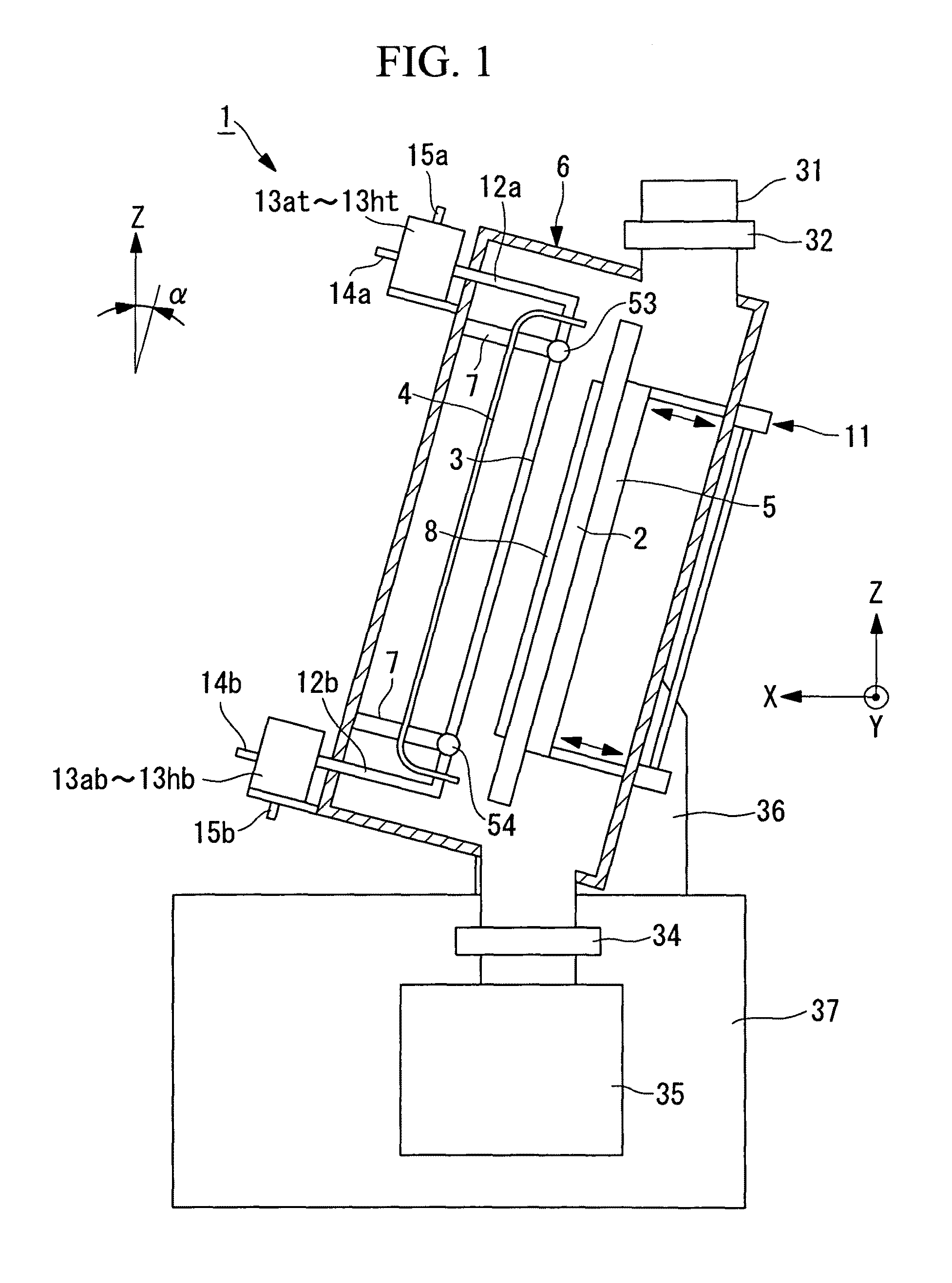
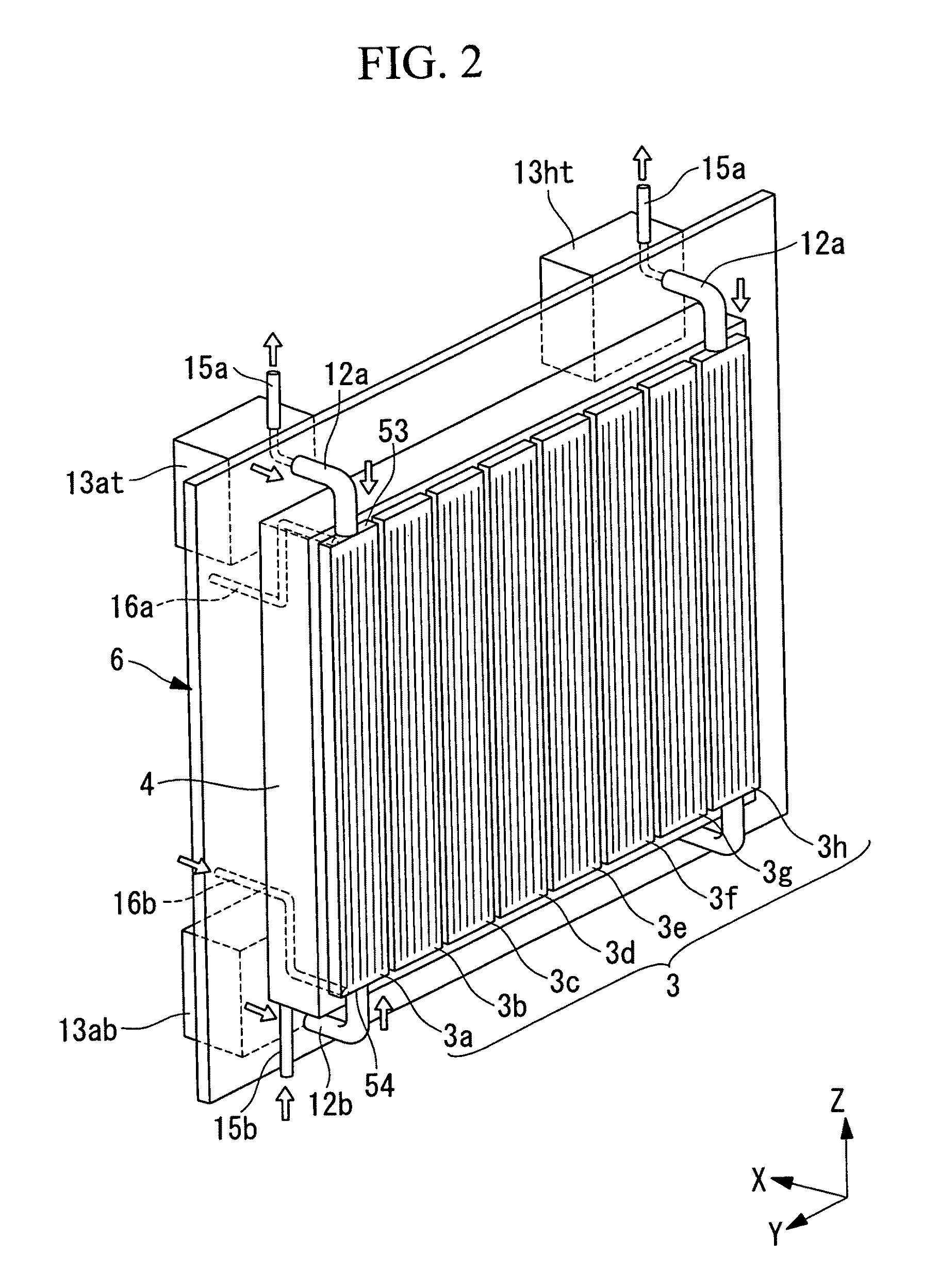
[0051]FIG. 1 shows a schematic view showing a configuration of a thin-film manufacturing apparatus of the embodiment, which is seen from a side of the thin-film manufacturing apparatus.

[0052]In the embodiment, the invention is described while being applied to a thin-film manufacturing apparatus that may perform high-speed deposition processing of a film, including amorphous silicon, microcrystalline silicon, silicon nitride, used for an amorphous solar cell, a microcrystalline solar cell, a TFT (Thin Film Transistor) for a liquid crystal display and the like under a high-pressure narrow-gap condition as a deposition condition, in which the deposition pressure is high and the discharge distance between an electrode and a substrate is narrow.

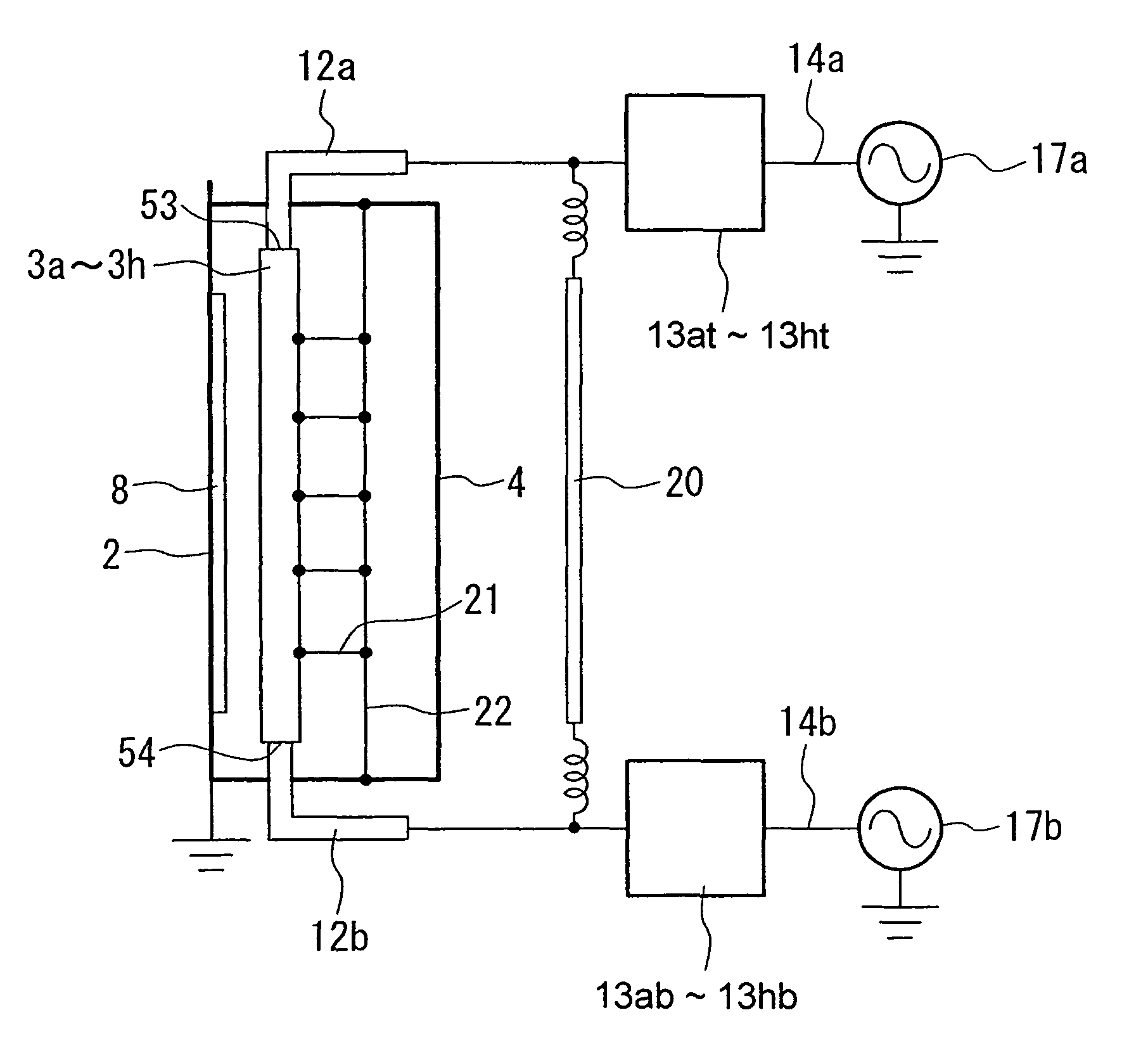
[0053]As shown in FIG. 1, a thin-film manufacturing apparatus (vacuum processing apparatus) 1 has a deposition chamber 6 being a vacuum vessel,...

second embodiment

[0118]Next, a second embodiment of the invention is described.

[0119]In a thin-film manufacturing apparatus of the embodiment, a basic configuration is the same as that of the first embodiment, but an impedance tuning method of a matching box is different from that of the first embodiment. Therefore, in the embodiment, only the impedance tuning method of a matching box is described, and description of other components and the like is omitted.

[0120]The same components as in the first embodiment are referenced by the same symbols, and a description thereof is omitted.

[0121]A tuning method of a thin-film manufacturing apparatus 1 of the embodiment is described.

[0122]First, a step of selecting a predetermined discharge electrode (here, description is made using a case that a discharge electrode 3b is selected), a step of determining an impedance value Z0 of each of representative matching boxes 13bt and 13bb, and a step that an impedance value of each of all matching boxes 13at, 13ct to ...

third embodiment

[0128]Next, a third embodiment of the invention is described.

[0129]In a thin-film manufacturing apparatus of the embodiment, a basic configuration is the same as that of the first embodiment, but an impedance tuning method of a matching box is different from that of the first embodiment. Therefore, in the embodiment, only the impedance tuning method of a matching box is described, and description of other components and the like is omitted.

[0130]The same components as in the first embodiment are referenced by the same symbols, and a description thereof is omitted.

[0131]A tuning method of a thin-film manufacturing apparatus 1 of the embodiment is described.

[0132]First, a step of selecting a predetermined discharge electrode (here, description is made using a case that a discharge electrode 3b is selected), a step of determining an impedance value Z0 of each of the representative matching boxes 13bt and 13bb, and a step in which the impedance values of all matching boxes 13at to 13ht ...


PUM

PropertyMeasurementUnit
widthaaaaaaaaaa
lengthaaaaaaaaaa
frequencyaaaaaaaaaa

Abstract

A vacuum processing apparatus is provided, in which a deposition characteristic is easily adjusted, and occurrence of difference in deposition characteristic between deposition chambers can be suppressed, and reduction in equipment cost can be achieved, and a deposition method using the vacuum processing apparatus is provided. The vacuum processing apparatus is characterized by having a plurality of discharge electrodes (3a to 3h) that are supplied with high-frequency power from a power supply unit (17a) through both ends (53) thereof, and form plasma with respect to a substrate (8) respectively, and a plurality of matching boxes (3a to 3ht) which tune phases and amplitudes of the high-frequency power supplied to the plurality of discharge electrodes (3a to 3h) at the ends (53) respectively; wherein impedance of the plurality of matching boxes (3a to 3ht) are set to approximately the same value, and the impedance value is a value at which reflected power is approximately minimized, the reflected power being returned to the power supply unit (17a) from one discharge electrode among the plurality of discharge electrodes (3a to 3h).

Description

TECHNICAL FIELD[0001]The present invention relates to a vacuum processing apparatus, and particularly relates to a vacuum processing apparatus that performs processing of a substrate by using plasma.BACKGROUND ART[0002]Recently, a plasma CVD apparatus using a plasma enhanced chemical vapor deposition (PCVD) method is used to deposit a material such as silicon onto a substrate having a large area (for example, at least 1 m in length and at least 1 m in width). The plasma CVD apparatus is used for deposition processing of a film including amorphous silicon, microcrystalline silicon, silicon nitride and the like used for, for example, an amorphous solar cell, a microcrystalline solar cell, and a TFT (Thin Film Transistor) for a liquid crystal display, and has a function of cleaning a film adhered on a chamber or a discharge electrode by etching (self-cleaning).[0003]As the discharge electrode of the plasma CVD apparatus, a discharge electrode including rod-like, longitudinal electrodes...

Claims


Application Information

Patent Timeline
Patent Type & Authority Patents(United States)
IPC IPC(8): C23C16/00H01L21/306C23F1/00C23C16/24C23C16/509H01J37/32H01L21/02
CPCC23C16/24C23C16/509H01J37/32091H01J37/32183H01L21/02532H01L21/0262
Inventor KAWAMURA, KEISUKEMASHIMA, HIROSHI
Owner MITSUBISHI HEAVY IND LTD
Why Eureka
Try Eureka