
Manufacture method of photovoltaic component device

A photovoltaic element and manufacturing method technology, applied in the direction of electrical components, final product manufacturing, sustainable manufacturing/processing, etc., can solve the problems of unloadable output current, short circuit of photovoltaic element devices, etc., and achieve the effect of improving photoelectric conversion efficiency

Inactive Publication Date: 2011-05-11
GALLANT PRECISION MACHINING CO LTD
View PDF0 Cites 0 Cited by
  • Summary
  • Abstract
  • Description
  • Claims
  • Application Information

AI Technical Summary

Problems solved by technology

However, after the P-type semiconductor substrate undergoes a phosphorous diffusion process, not only the N-type semiconductor layer is formed on one surface, but the N-type semiconductor layer will also cover the surrounding surface and include the On all sides of the P-type semiconductor layer, therefore, the N-type semiconductor film on all these sides must be removed, otherwise it will cause a short circuit of the photovoltaic device and fail to output current to the load

Method used

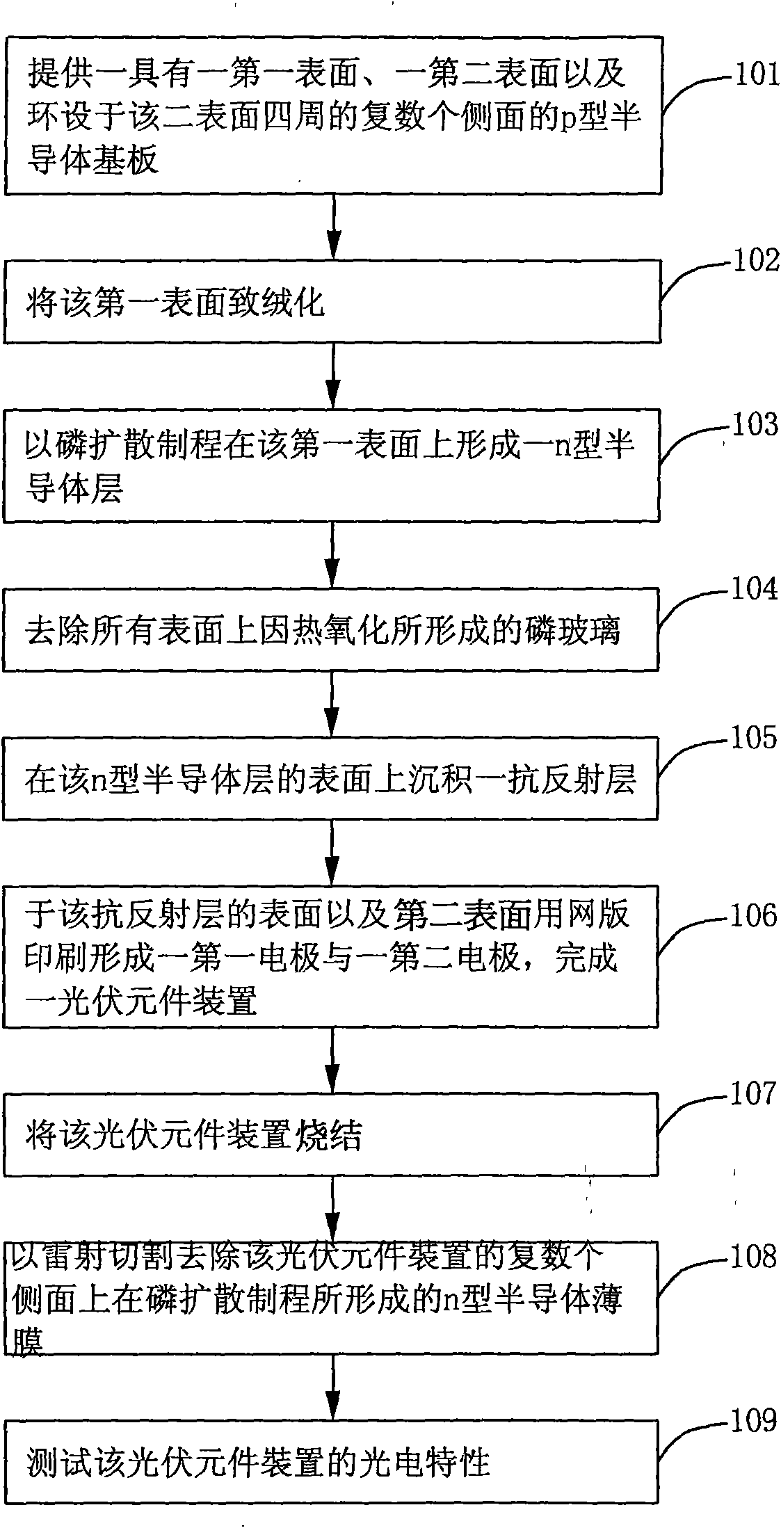
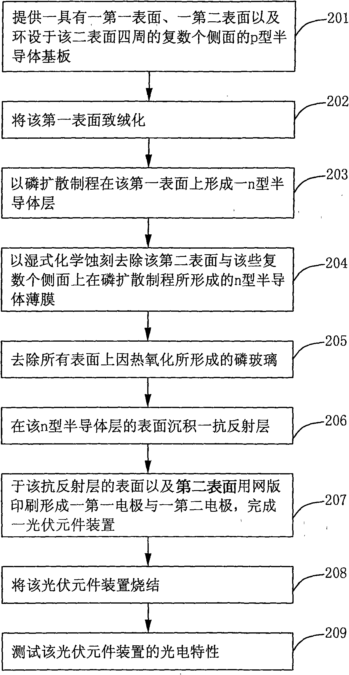
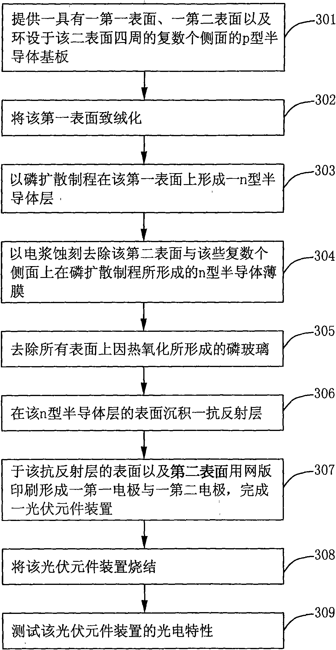

Image

  • Manufacture method of photovoltaic component device
  • Manufacture method of photovoltaic component device
  • Manufacture method of photovoltaic component device

Examples


Embodiment Construction

[0098] In order to enable your examiner to have a further understanding and understanding of the characteristics, purpose and functions of the present invention, the relevant detailed structure and design concept of the present invention will be explained below, so that the examiner can understand the characteristics of the present invention , the detailed statement is as follows:

[0099] see Figure 4A As shown, the figure is a schematic diagram of the manufacturing process of the photovoltaic element device using the mask layer insulation method according to the first embodiment of the present invention. As shown in the figure, the manufacturing process of the photovoltaic element device in this embodiment includes the following steps:

[0100] Step 401: providing a first-type semiconductor substrate having a first surface, a second surface, and a plurality of side surfaces surrounding the two surfaces;

[0101] Step 402: Texturing the first surface;

[0102] Step 403: f...


PUM


Abstract

The present invention provides a manufacture method of photovoltaic component device, wherein a P-type semiconductor basal plate is provided; the basal plate has a first surface, a second surface and a plurality of side faces annularly disposed around the two surfaces. After the first surface is flocked, a shading layer is formed on the second surface and the side faces, so that when the basal plate is in a phosphorus diffusion process, a N-type semiconductor layer only can be formed on the first surface.

Description

technical field [0001] The present invention relates to a method for manufacturing a photovoltaic element device, in particular to a method for forming a mask layer on the surface of a silicon substrate of a photovoltaic element device, so that when the substrate is subjected to a diffusion process to form a PN junction diode , will not cause the short circuit of the PN junction diode on its side. Background technique [0002] In recent years, the global warming caused by the greenhouse effect has become the most important issue in the world. The development of clean energy is an inevitable trend, and solar energy is the focus of renewable energy technology development. Because the photovoltaic element device uses the principle of the photoelectric effect to generate electricity, since no carbon dioxide is generated during the power generation process, it will make a great contribution to slowing down the global warming effect. [0003] Among various photovoltaic device dev...

Claims


Application Information

Patent Timeline
Patent Type & Authority Applications(China)
IPC IPC(8): H01L31/18
CPCY02P70/50
Inventor 王宗薪陈来成郑铁扉洪伸锜粘守裕杜信璋林汉斌徐享桢顾乃桓林育圣林明辉
Owner GALLANT PRECISION MACHINING CO LTD
Learn More