

Limiter circuit
A limiter circuit and a limiter technology, which are applied in the direction of limiter, diode limiter, non-control loop limiter, etc., can solve the problem of increasing structural components of the limiter circuit, circuit complexity, etc., to achieve limiter action, simple The effect of circuit structure
- Summary
- Abstract
- Description
- Claims
- Application Information
AI Technical Summary
Problems solved by technology
Method used
Image

Examples
Embodiment 1
[0039] Hereinafter, Embodiment 1 of the present invention will be described in detail with reference to the drawings.
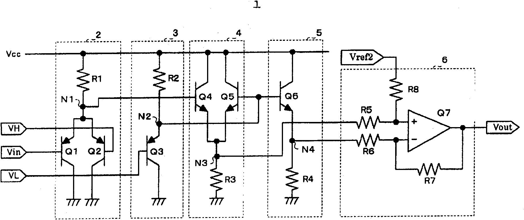
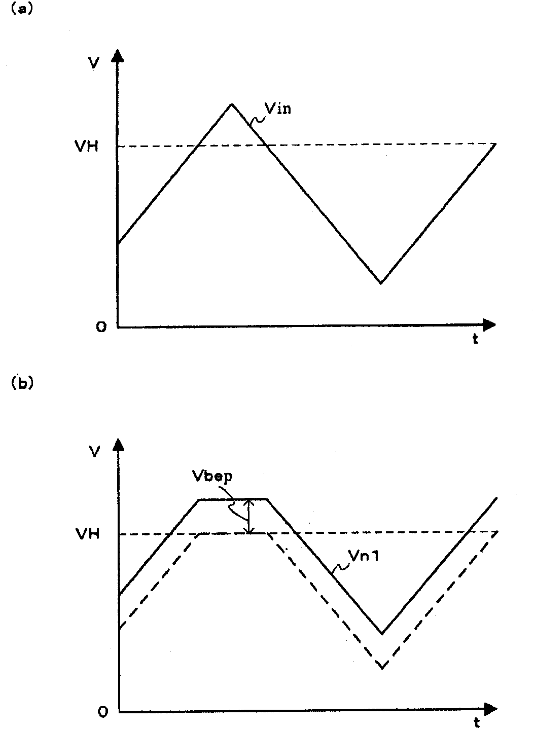
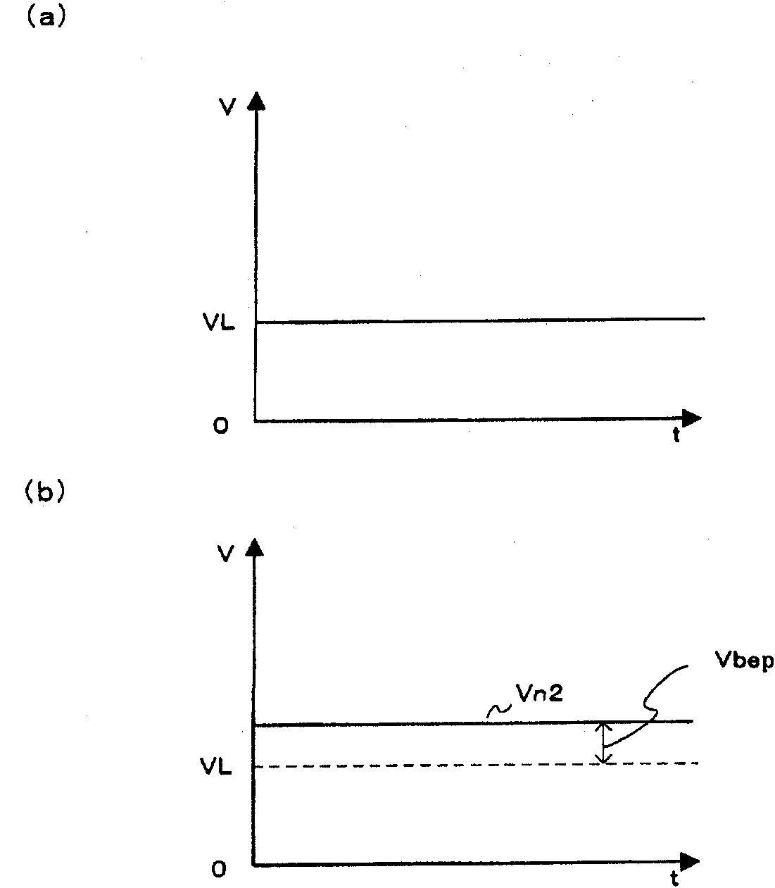
[0040] figure 1 is a circuit diagram showing the clipping circuit of the first embodiment. The limiter circuit of the present invention is configured inside an IC such as an input buffer amplifier of an analog / digital converter or a signal processing circuit, for example.
[0041] Such as figure 1 As shown, the limiter circuit 1 of Embodiment 1 includes: a switch circuit 2, which controls on and off according to the magnitude relationship between the input signal Vin and the upper threshold signal VH; the lower limit threshold correction circuit 3, which will follow the switching circuit 2 is controlled by the switch and the boosted potential is corrected as the lower limit threshold signal VL; the switch circuit 4 controls on and off according to the magnitude relationship between the output of the switch circuit 2 and the lower limit threshold correctio...
Embodiment 2
[0136] Next, refer to Figure 8 and Figure 9 Embodiment 2 of the present invention will be described in detail.
[0137] Figure 8 is a circuit diagram showing the clipping circuit of Embodiment 2, Figure 9 It is an explanatory diagram for explaining the operation of the limiter circuit of the second embodiment.
[0138] Such as Figure 8 As shown, the limiter circuit 10 of Embodiment 2 includes: a switch circuit 2, which controls the turn-on and cut-off according to the magnitude relationship between the input signal Vin and the upper threshold signal VH; the lower limit threshold correction circuit 3, which generates the following The switch control of the switch circuit 2 and the boosted potential correction is the potential of the lower limit threshold signal VL; the switch circuit 4 controls the conduction and cut-off according to the magnitude relationship between the output of the switch circuit 2 and the lower limit threshold correction circuit 3; and adding The...
Embodiment 3
[0197] Next, refer to Figure 10 and Figure 11 Embodiment 3 of the present invention will be described in detail.
[0198] Figure 10 is a circuit diagram showing the limiter circuit of Embodiment 3, Figure 11 It is an explanatory diagram for explaining the operation of the limiter circuit of the third embodiment.
[0199] The limiter circuit 20 of Embodiment 3 includes: a switch circuit 21, which controls the turn-on and cut-off according to the magnitude relationship between the input signal Vin and the lower limit threshold signal VL; a potential correction circuit 22, which is used to correct the voltage drop caused by the switch circuit 21 and the addition and subtraction circuit 23, which differentially amplifies the outputs of the switch circuit 21 and the potential correction circuit 21. The switch circuit 21 corresponds to the lower limit limiter circuit in the present invention.
[0200] The limiter circuit 20 in the third embodiment performs only the lower li...
PUM
 Abstract
Description
Claims
Application Information