
A solder mask ink coating method

A solder mask ink and coating technology, applied in the application of non-metallic protective layer, secondary treatment of printed circuits, etc., can solve the problems of insufficient ink thickness at the corner of the line, line cavitation, etc., to avoid insufficient ink thickness, increase Fluidity, the effect of improving cavitation between lines

Inactive Publication Date: 2011-05-25
PEKING UNIV FOUNDER GRP CO LTD +1
View PDF0 Cites 45 Cited by
  • Summary
  • Abstract
  • Description
  • Claims
  • Application Information

AI Technical Summary

Problems solved by technology

[0003] The embodiment of the present invention provides a method for coating solder resist ink, which is used to solve the problem in the prior art that due to the thick copper layer, in the process of solder resist ink coating, the ink thickness at the corners of the circuit is prone to insufficient ink thickness, and the circuit The problem of air bubbles between

Method used


Image

  • A solder mask ink coating method
  • A solder mask ink coating method

Examples


Embodiment Construction

[0024] The specific implementation of a method for coating solder resist ink provided by the present invention will be described in detail below.

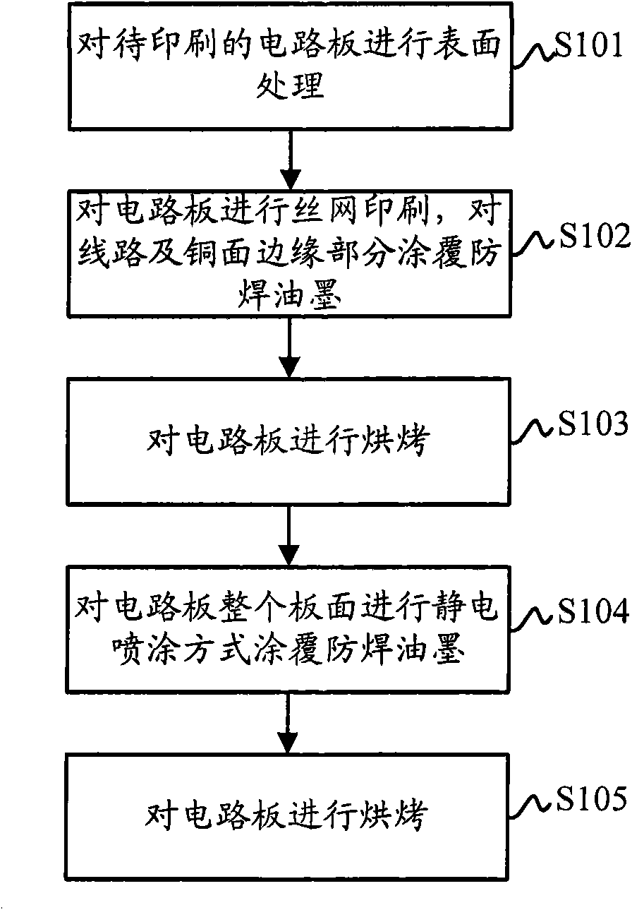
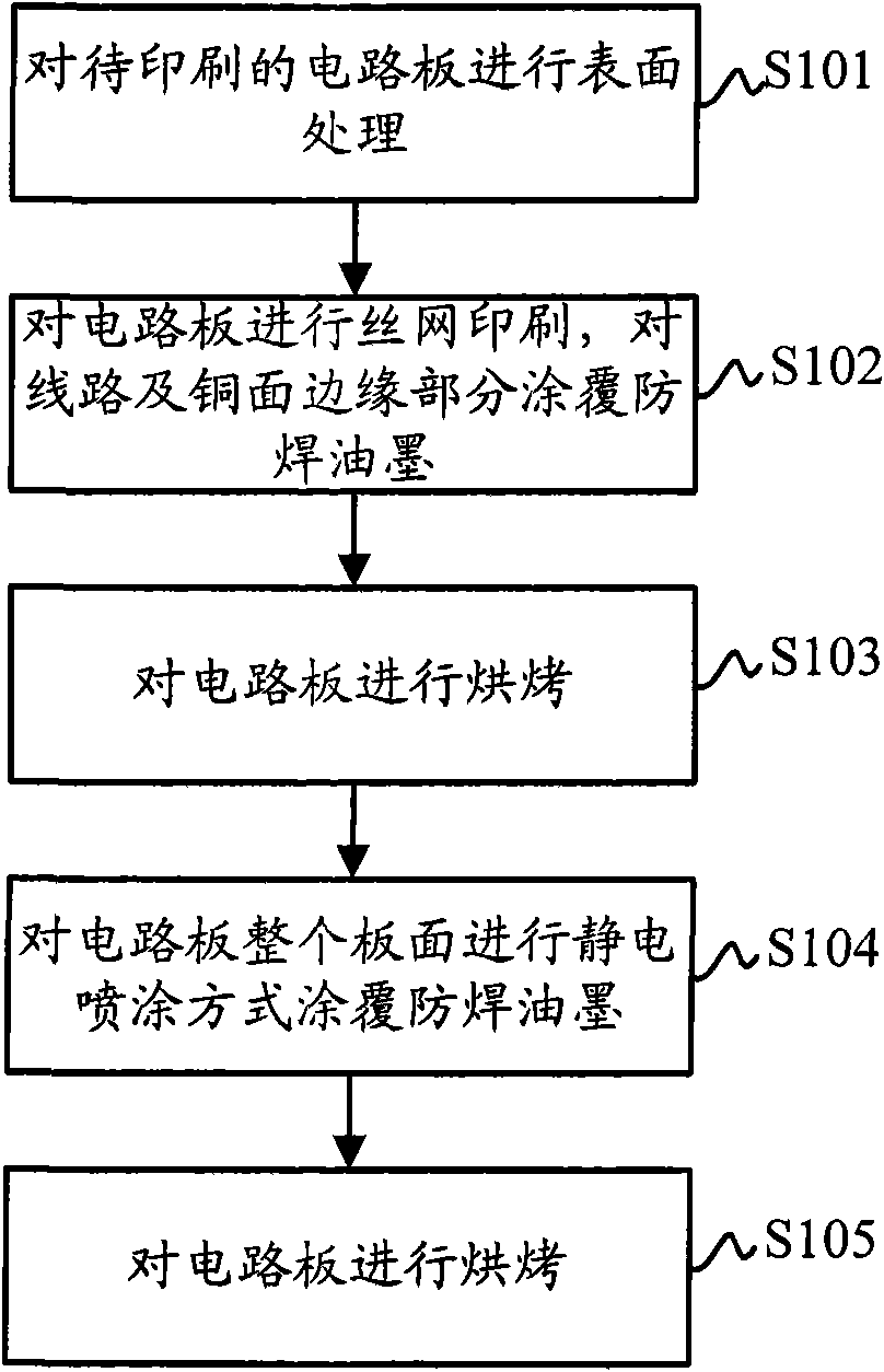
[0025] The coating method of the solder resist ink provided by the embodiment of the present invention comprises the following steps:

[0026] Surface treatment of circuit boards to be printed;

[0027] Cover the screen plate on the surface-treated circuit board, and screen-print the circuit board and the edge of the copper surface to coat the solder resist ink;

[0028] The entire layout of the screen-printed circuit board is again coated with solder resist ink.

[0029] The coating method of the solder resist ink provided in the embodiment of the present invention will be described in detail below with a specific example.

[0030] In this example, before the process of coating the solder resist ink on the circuit board, it is necessary to complete the preparation of corresponding tools and materials, such as the design and prod...


PUM


Abstract

The invention discloses a solder mask ink coating method which comprises the following steps: laying a screen printing plate over a circuit board which has been given a surface treatment; conducting screen printing coating on the circuit board lines and on the marginal portion of the copper surface; and conducting solder mask ink coating on the whole plate surface of the circuit board which have been given screen printing coating. The solder mask ink coating method provided by the present invention can conduct two separate solder mask ink coatings on the circuit board lines and the copper surface marginal portion; for those circuit boards with relatively thick copper layers, the invention can effectively avoid the problems of insufficient printing oil ink thickness at the line corners and the generation of cavity between the lines and can enhance the product reliability.

Description

technical field [0001] The invention relates to the field of circuit board manufacturing, in particular to a method for coating solder resist ink. Background technique [0002] Today, when printed circuit board (PCB) products are widely used, as an indispensable branch of PCB, PCB with thick copper plate (copper thickness ≥ 3OZ) still has a place, and its manufacturing process is complex and difficult to produce. , especially the production of the solder resist ink layer covered on its surface, there have been many quality problems. Due to the thick copper thickness of the circuit board, in the process of coating the solder resist ink, the ink thickness at the corners of the circuit is prone to insufficient ink thickness, and cavitation occurs between the lines, which affects the appearance of the product. Moreover, after the circuit board is subjected to high temperature During the soldering process, if the ink thickness at the corners of the lines is insufficient, and if ...

Claims


Application Information

Patent Timeline
IPC IPC(8): H05K3/28
Inventor 徐学军胡誉苏新虹
Owner PEKING UNIV FOUNDER GRP CO LTD
Features
  • Generate Ideas
  • Intellectual Property
  • Life Sciences
  • Materials
  • Tech Scout
  • Unparalleled Data Quality
  • Higher Quality Content
  • 60% Fewer Hallucinations
Learn More