Check patentability & draft patents in minutes with Patsnap Eureka AI!

Thin film transistor array substrate, light-emitting panel and manufacturing method thereof as well as electronic device

A thin-film transistor and light-emitting panel technology, which is applied in semiconductor/solid-state device manufacturing, circuits, electrical components, etc., can solve the problems of reduced manufacturing pass rate, increased influence of particles, and the probability of particle point defects, etc.

Inactive Publication Date: 2011-06-01
CASIO COMPUTER CO LTD
View PDF4 Cites 6 Cited by
  • Summary
  • Abstract
  • Description
  • Claims
  • Application Information

AI Technical Summary

Problems solved by technology

[0007] However, the more film formation and patterning processes, the easier it is to generate particles (fine foreign matter) on the substrate, so the remaining particles short-circuit the positive electrode and the negative electrode, and point defects occur, reducing the manufacturing yield (increasing the defective rate).
That is, when comparing the liquid crystal element structure and the organic EL element structure, since the light-emitting functional layer in the organic EL element is much thinner than the liquid crystal layer in the liquid crystal element, the probability of occurrence of point defects in particles becomes high.
In addition, as mentioned above, when it is desired to increase the image quality of the display panel and increase the size of the screen, the influence of particles is relatively large.

Method used


Image

  • Thin film transistor array substrate, light-emitting panel and manufacturing method thereof as well as electronic device
  • Thin film transistor array substrate, light-emitting panel and manufacturing method thereof as well as electronic device
  • Thin film transistor array substrate, light-emitting panel and manufacturing method thereof as well as electronic device

Examples


Embodiment Construction

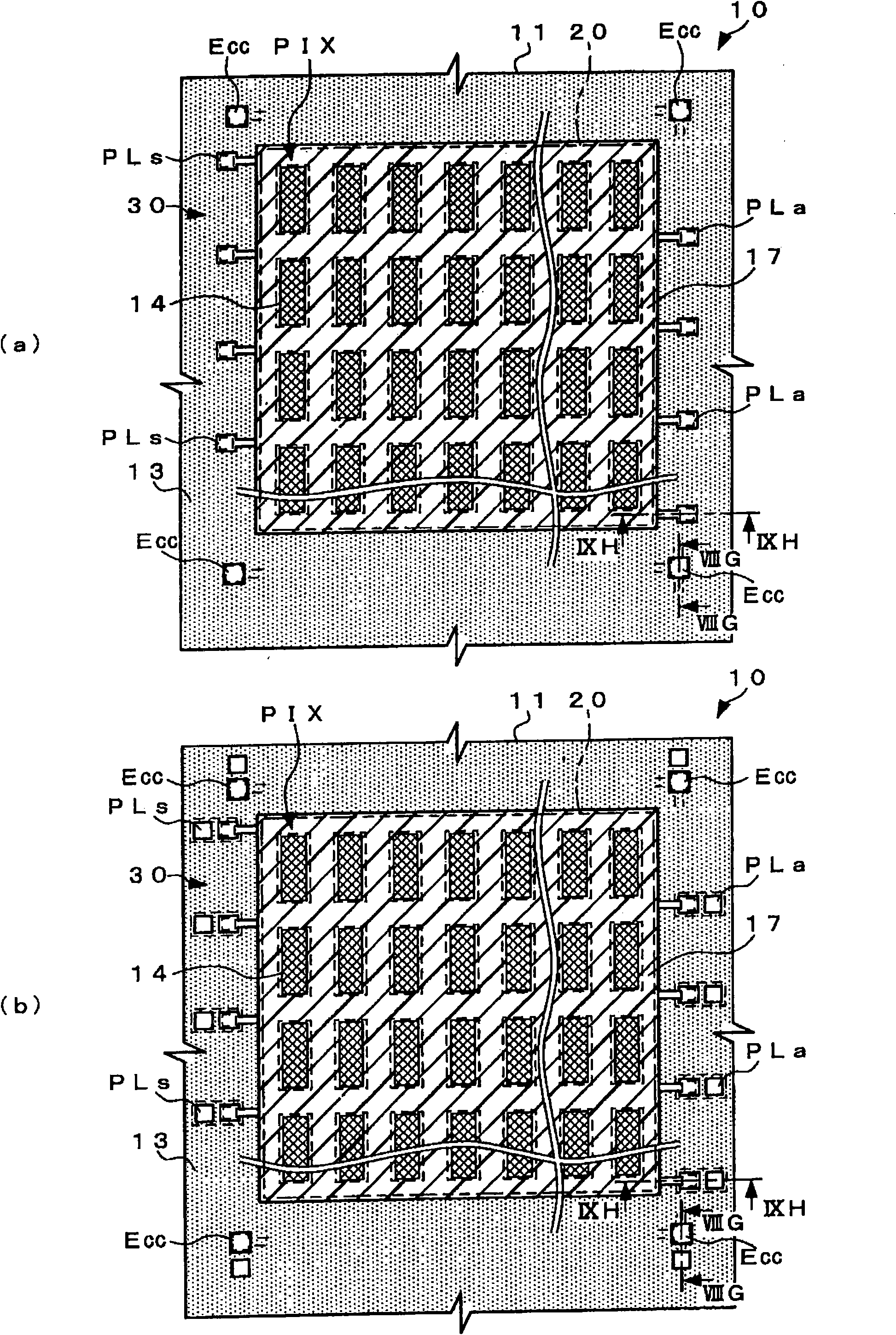
[0028] Hereinafter, the thin film transistor array substrate, the light-emitting panel, the manufacturing method thereof, and the electronic device according to the embodiments will be described in detail by showing the embodiments. First, a light emitting panel to which the thin film transistor array substrate of the embodiment and its manufacturing method are described. Here, a display panel in which a plurality of pixels including organic EL elements are arrayed will be described as a light emitting panel to which the thin film transistor array substrate of the embodiment is applied.

[0029] (luminescent panel)

[0030] figure 1 A. figure 1 B is a schematic plan view showing an example of a display panel to which the thin film transistor array substrate of the embodiment is applied. figure 1 A is a schematic plan view showing a first example of a display panel, figure 1 B is a schematic plan view showing a second example of the display panel. also, figure 2 is showi...


PUM


Abstract

The invention provides a thin film transistor array substrate, a light-emitting panel and a manufacturing method thereof as well as an electronic device. A thin film transistor array substrate includes a substrate, thin film transistors formed on the substrate, wirings provided on the substrate. The wirings are subjected to an application of a voltage to drive circuits including the thin film transistors. At least part of the surface of each of the wirings is made of an anodic oxide film.

Description

[0001] This application is based on Japanese Patent Application No. 2009-226156 filed on September 30, 2009, and the priority of this earlier application is claimed, and all the contents of this earlier application are incorporated in this application. technical field [0002] The invention relates to a thin film transistor array substrate, a light-emitting panel, a manufacturing method thereof, and electronic equipment. Background technique [0003] In recent years, as a display device of electronic equipment such as a mobile phone or a portable music player, a device using a display panel in which a light-emitting element such as an organic electroluminescent element (hereinafter, simply referred to as "organic EL element") is widely known Dimensionally arranged display panel (light-emitting element type display panel). In particular, in the light-emitting element type display panel to which the active matrix driving method is applied, compared with the widely used liquid ...

Claims


Application Information

Patent Timeline
Patent Type & Authority Applications(China)
IPC IPC(8): H01L27/12H01L27/32H01L51/56
CPCH01L27/3276G09G3/3233G09G2300/0861H01L27/12H01L27/124H10K59/131H10K50/844
Inventor 东俊明
Owner CASIO COMPUTER CO LTD
Features
  • R&D
  • Intellectual Property
  • Life Sciences
  • Materials
  • Tech Scout
  • Unparalleled Data Quality
  • Higher Quality Content
  • 60% Fewer Hallucinations
Learn More