Exponential-doping GaN ultraviolet photocathode material structure and preparation method thereof
A technology of exponential doping and cathode materials, applied in cold cathode manufacturing, electrode system manufacturing, discharge tube main electrode, etc., can solve problems such as weak theoretical support, not too suitable concentration and thickness, inconvenient theoretical simulation and data optimization, etc. , to achieve the effect of facilitating theoretical design, improving the overall quantum efficiency, and increasing the escape depth
- Summary
- Abstract
- Description
- Claims
- Application Information
AI Technical Summary
Problems solved by technology
Method used
Image
Examples
Embodiment 1
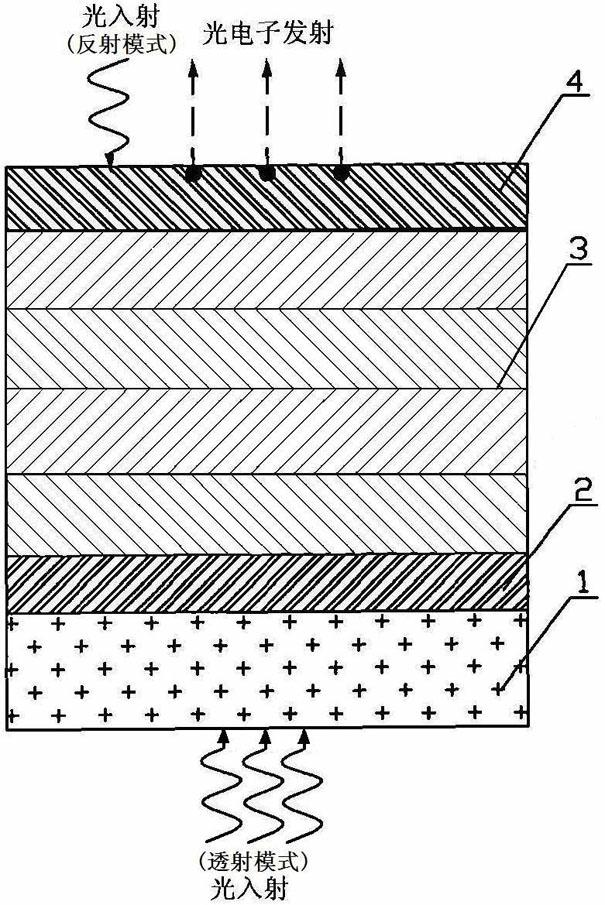
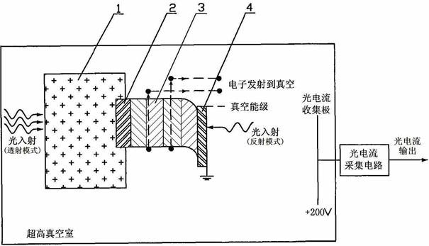
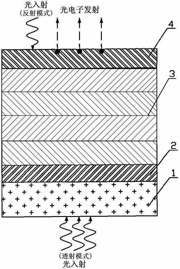
[0028] Embodiment 1: as figure 1 As shown, a GaN ultraviolet photocathode material structure, the material structure consists of a substrate 1 (such as sapphire), an unintentionally doped AlN buffer layer 2, a p-type exponentially doped GaN photoemissive layer 3, and Cs or The Cs / O active layer 4 is composed; wherein, the unintentionally doped AlN buffer layer 2 is epitaxially grown on the substrate layer 1 with a thickness of 50nm; the p-type index-doped GaN photoemissive layer 3 is epitaxially grown on the aforementioned AlN buffer layer 2 , with a thickness of 185nm and a doping concentration of 1×10 18 cm -3 , 2.35×10 17 cm -3 , 1.19×10 17 cm -3and 6×10 16 cm -3 , gradually decreases exponentially from the body to the body surface; the Cs or Cs / O active layer 4 is adsorbed on the front surface of the p-type exponentially doped GaN photoemissive layer 3 through an ultra-high vacuum activation process, with a thickness of one monoatomic layer.
Embodiment 2
[0029] Embodiment 2: Different from Embodiment 1, the thickness of the AlN buffer layer is 100nm; the p-type exponentially doped GaN photo-emitting layer 3 is epitaxially grown on the aforementioned AlN buffer layer 2, with a thickness of 185nm and a doping concentration of 1× 10 18 cm -3 , 2.35×10 17 cm -3 , 1.19×10 17 cm -3 and 6×10 16 cm -3 , gradually decreases exponentially from the body to the body surface; the Cs or Cs / O active layer 4 is adsorbed on the front surface of the p-type exponentially doped GaN photoemissive layer 3 through an ultra-high vacuum activation process, with a thickness of one monoatomic layer.
Embodiment 3
[0030] Embodiment 3: Different from Embodiment 1, the thickness of the AlN buffer layer is 50nm; the p-type exponentially doped GaN photo-emitting layer 3 is epitaxially grown on the aforementioned AlN buffer layer 2, with a thickness of 200nm and a doping concentration of 1× 10 18 cm -3 , 2.99×10 17 cm -3 , 1.34×10 17 cm -3 and 6×10 16 cm -3 , gradually decreases exponentially from the body to the body surface; the Cs or Cs / O active layer 4 is adsorbed on the front surface of the p-type exponentially doped GaN photoemissive layer 3 through an ultra-high vacuum activation process, with a thickness of one monoatomic layer.
PUM
| Property | Measurement | Unit |
|---|---|---|
| Thickness | aaaaa | aaaaa |
| Thickness | aaaaa | aaaaa |
| Thickness | aaaaa | aaaaa |
Abstract
Description
Claims
Application Information


