Method of fabricating high-k/metal gate device

A high-k dielectric and metal gate technology, applied in the field of manufacturing high-k dielectric layers and/or metal gate components, can solve the problems of high-k gate dielectric layer quality degradation and achieve Improved etching process, cost-effective effect

Active Publication Date: 2011-06-22
TAIWAN SEMICON MFG CO LTD
View PDF3 Cites 25 Cited by
  • Summary
  • Abstract
  • Description
  • Claims
  • Application Information

AI Technical Summary

Problems solved by technology

In view of this, in the CMOS technology manufacturing process, one or more thermal process cycles (such as dummy polysilicon thermal step,

Method used


Image

  • Method of fabricating high-k/metal gate device
  • Method of fabricating high-k/metal gate device
  • Method of fabricating high-k/metal gate device

Examples


Embodiment Construction

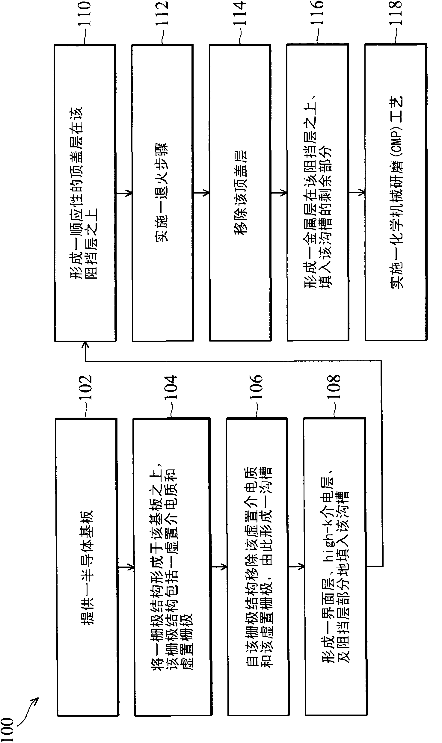
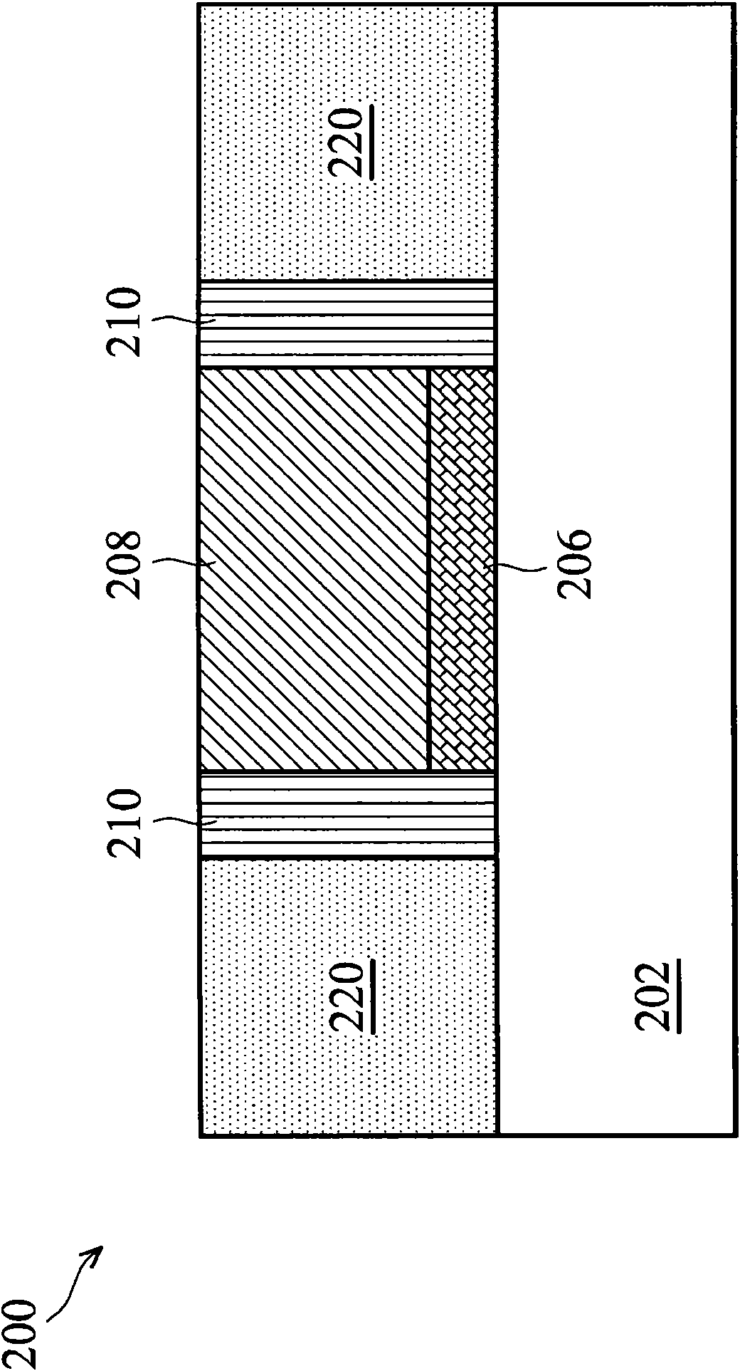
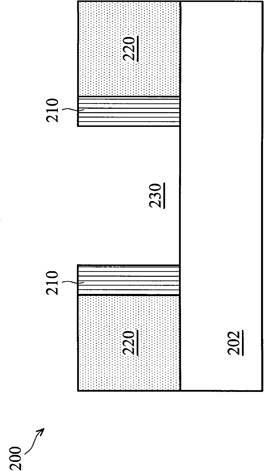
[0036] In order to make the present invention more comprehensible, the following specific embodiments are described in detail in conjunction with the accompanying drawings as follows:

[0037] Hereinafter, each embodiment is described in detail and examples accompanied by drawings are used as a reference basis of the present invention. In the drawings or descriptions of the specification, the same reference numerals are used for similar or identical parts. And in the drawings, the shapes or thicknesses of the embodiments may be enlarged, and marked for simplicity or convenience. Furthermore, the parts of each element in the drawings will be described separately. It should be noted that the elements not shown or described in the drawings are forms known to those skilled in the art. In addition, specific embodiments only The specific method used in the present invention is disclosed, and it is not intended to limit the present invention. Furthermore, embodiments of the "gate-l...


PUM

PropertyMeasurementUnit
Thicknessaaaaaaaaaa

Abstract

The present disclosure provides a method that includes providing a semiconductor substrate; forming a gate structure over the semiconductor substrate, first gate structure including a dummy dielectric and a dummy gate disposed over the dummy dielectric; removing the dummy gate and the dummy dielectric from the gate structure thereby forming a trench; forming a boundary layer on the semiconductor substrate; forming a high-k dielectric layer on the boundary layer partially filling the trench; forming a barrier layer over the high-k dielectric layer partially filling the trench; forming an capping layer over the barrier layer partially filling the trench; performing an annealing process; removing the capping layer; forming a metal layer over the barrier layer filling in a remainder of the trench; and performing a chemical mechanical polishing (CMP) to remove the various layers outside the trench. The invention can improve the quality of the high-k dielectric layer in the final component.

Description

technical field [0001] The invention relates to a method for manufacturing a semiconductor element, in particular to a method for manufacturing a high-permittivity dielectric layer and / or a metal gate element. Background technique [0002] The semiconductor integrated circuit (IC) industry has experienced rapid growth. Technological advances in IC materials and design have resulted in the evolution of generations of ICs, each with smaller and more complex circuits than the previous generation. However, the aforementioned advancements have increased the complexity of manufacturing ICs and processes, and in order for these advanced technologies to be realized, the development of similar IC processes and fabrications is necessary. [0003] In the course of IC evolution, the density of functions (i.e., the number of devices interconnected per chip area) has gradually increased, while the geometry size (i.e., the smallest element (or line) that can be created using a process) ha...

Claims


Application Information

Patent Timeline
IPC IPC(8): H01L21/28H01L21/283
CPCH01L29/4966H01L21/28088H01L21/28194H01L29/66545H01L29/517H01L21/28185
Inventor 李达元许光源于雄飞李威养叶明熙
Owner TAIWAN SEMICON MFG CO LTD
Why Eureka
Try Eureka